This service is accessible for all EUROPRACTICE customers. It is provided by our partner Fraunhofer.
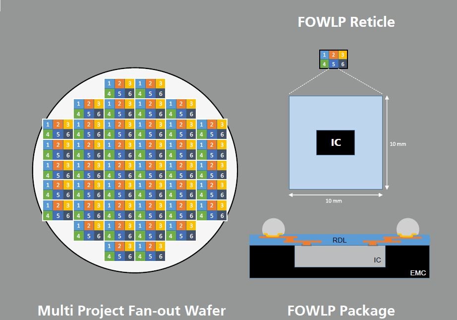
| Design Rules & Materials | Multi-project wafer processing is an established approach in semiconductor manufacturing for fast and low-cost prototyping. This idea is now transferred to fan-out wafer level packaging. Here dies from different sources or different technologies with varying thickness and size can be handled and packaged with one integration technology. This offers a path to a well adopted technology, especially for RF applications. |
| MPFOWL Package Specification | Die delivery: WafflePack, wafer, wheel Die size: 1.5 – 7 mm edge length Die thickness: 200 – 300 μm Package thickness: 450 μm Package size: 10×10 mm², smaller package size possible with extra effort Metal layers: 2 Integration of e.g. antennas and passive structures in RDL Pin-out: BGA - Pitch: 500 μm - Ball size: 300 μm - Solder: SnAgCu Defined packaging materials |
You can find more details in the MPFOWLP flyer
Contact
Dr. Tanja Braun
e-mail: europractice@izm.fraunhofer.de
Fraunhofer Institute for Reliability and Microintegration IZM
Gustav-Meyer-Allee 25
13355 Berlin, Germany
www.izm.fraunhofer.de
CMP, in partnership with CEA-LETI, offers a set of post-processes allowing various types of 3D assemblies.
These wafer-level services are available only for the customers of the EUROPRACTICE partner CMP.
Those post-processes are operated at wafer-level and are carried out after standard MPW runs on a selected subset of technologies. The goal is to integrate 3D interconnections to chips processed through CMP, in order to enable flip-chip on organic or ceramic substrates as well as Die-to-Die or Die-to-Interposer assemblies.
Two types of post-processes are available, including different options:
Technology characteristics:
| µBumps (Cu-pillar) | Cu/SnAg ; ø25 µm ; 50 µm min pitch ; ~20 µm thickness |
| UBM | TiNiAu ; 25 µm min width; 50 µm min pitch ; 1 µm thickness |
| TSV-LAST | Ø60 µm x 120 µm depth ; 120 µm min pitch |
| Backside RDL | Cu ; 20 µm min width ; 40 µm min pitch ; 4-8 µm Thickness |
Accessibility conditions:
MPW OPEN 3D post processes are available for projects and wafers processed through CMP on the last CMP MPW run of the year for the following technologies:
| ams | C35B4M3 |
| CEA-LETI | Silicon Photonics |
| STMicroelectronics | CMOS28FDSOI (frontside only), BiCMOS055, CMOS065, BiCMOS9MW |
Those runs are subject to a certain minimum number of participants sharing the MPW.
MPW OPEN 3D post‐processes must be anticipated at an early stage as they require an additional NDA, the distribution of a specific DRM and an add‐on to the Design‐Kit. Additionaly, this must be indicated it in the reservation form.
Dedicated OPEN3D post processes can be made available on any CMP MPW Run at any time of the year after a feasibility study. In this case, restrictions to specific geometrical parameters of the design structure are not imposed and can be chosen within a process window. Please contact CMP for more information/quotation.
Application area:
3D/2.5D integration
Design kit version:
CMP/LETI 3D add-on is required to design post-processed modules
Verification tools:
DRC calibre die-level; DRC calibre 3Dstack for assembly-level checks (at CMP only)
Libraries:
3D modules Library
Packaging:
OPEN 3D post processing is available upon request, please contact ajith-sivadasan.moreau@mycmp.fr for more information on packaging solutions.
Fraunhofer and CMP provide access to this ams technology.
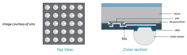
| Technology characteristics | Solder bumping consists in manufacturing metal spheres acting as interconnections for flip-chip. Those spheres are composed of a Sn/Ag/Cu alloy (SAC). Before the sphere can be deposited, the deposition of an Under Bump Metalization (UBM) layer is required. This option, available on ams 0.35 & 0.18 runs only, is operated at wafer-level within ams cleanroom after CMOS process. It allows the deposition of an array of solder balls at wafer-level, with an I/O pitch compatible with traditional printed circuit board (PCB) assembly processes. For mechanical reasons solder balls are usually evenly distributed over the whole chip surface and electrically connected to the IC‘s CMOS pads by means of a redistribution layer (RDL) included in the option. |
| Application area | Single die flip-chip packaging |
| Design Kit version | Option supported by ams hitkit 4.10 ISR15, through an add-on |
This technology is provided by CMP. Copper pillars are manufactured at wafer-level by STMicroelectronics. This interconnection is composed of an Under Bump Mettalization (UBM), upon which a pillar of copper is grown, a capping of Sn/Ag allows the die to be assembled on a substrate by reflow process. The dimensions of this copper pillar are approximately 62 µm in diameter for 65 µm in height, thus allowing a fine pitch (down to 90 µm).
Accessibility conditions:
More detailed techical information is available on the CMP website.