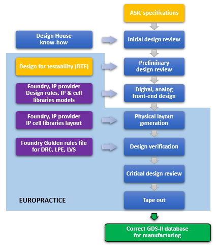
When working on the ASIC design, customers receive support from EUROPRACTICE with test insertion and ATPG (Automated Test Pattern Generation) to get the highest test coverage. Important know-how from the test house is used to improve the DFT (Design For Testability). As soon as a preliminary layout of the ASIC is ready, EUROPRACTICE can also provide technical support regarding the choice of package type and assembly requirements.
During the tape-out procedure, all circuits are checked against design rule violations with the “golden rule files” from the foundry. As a result, a correct GDS-II database is delivered to the foundry where the prototypes will be fabricated.
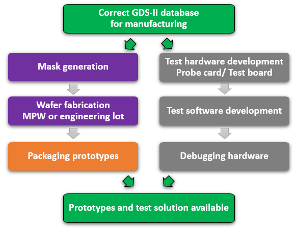
After all the checks have been performed and the GDS-II database is ready for production, the foundry can generate masks and produce prototypes via the EUROPRACTICE MPW (Multi Project Wafer) runs or SPW (Single Project Wafer) runs. If required, the resulting prototypes can be packaged by one of the assembly houses within Europe or in the Far East.
In parallel with the wafer production, the test solution is developed. The ASICs can be tested on both wafer level as well as packaged devices.
When packaged prototypes are available, they are shipped to the test house for debugging.This procedure includes continuity and leakage tests, the ATPG (Automated Test Pattern Generation) and testing of all analog blocks (when available on the ASIC) at room temperature (RT). When the ASIC is working according to the specifications, further tests are performed at low and high temperature (LT and HT).
The next stage is a full characterization of the ASIC at the edges of the power supply range and frequency at LT, RT and HT.
During each test, data logs of the measured values are generated and histograms are sent to the customer together with Cpk data. If required, a failure analysis is performed to understand the reason of the problem.
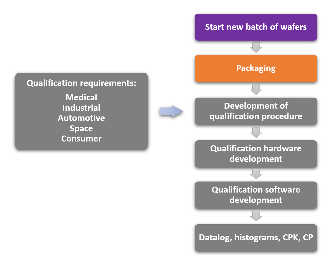
When customers only need prototypes of the ASIC, qualification is not needed. However, when prototypes are working correctly and the customer would like to scale up to volume production, it is the right time to think about the “product qualification”.
EUROPRACTICE offers a full qualification service provided by one of the test house partners. The qualification procedure can range from Consumer, Industry or Medical to Space qualification according to Military and JEDEC standards.
To speed up the procedure, most of the tests are run in parallel. In this stage of the project, qualification boards are developed for reliability and environmental testing.
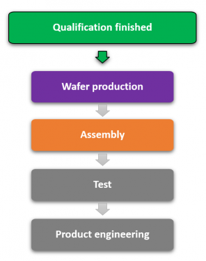
Once the ASIC has been qualified, it is ready for volume production. During the ramp-up phase, production and yield are closely monitored.
When the ASIC runs into higher volumes, it becomes reasonable to work on a cost down of the test solution. In this case, the test boards are copied and the originals remain in the developing test house for further monitoring while the copies are distributed to high volume test houses.
Legend:
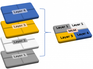
Together with Multi Project Wafer (MPW), EUROPRACTICE uses the Multi Layer Mask (MLM) technique to reduce fabrication costs.
In this case, the available mask area is typically divided in four quadrants (4L/R : four layer per reticle) whereby each quadrant is filled with one design layer. As an example, one mask can contain four layers such as nwell, poly, ndiff and active. The total number of masks is thus reduced by a factor of four. By adapting the lithographical procedure, it is possible to use one mask four times for the different layers by using the appropriate quadrants. Due to this technique, the mask costs can be reduced by approximately 60%.
These are some of the advantages of a MLM run:
The MLM technique is preferred over MPW runs when the chip area becomes large and when the customer wants to get a higher number of prototypes. If the prototypes are successful, the mask set can be used under certain conditions for low volume production.
MLM runs are only available for technologies from ON Semiconductor, IHP, GLOBALFOUNDRIES and XFAB.