SYSTEM & CHIPLET INTEGRATION

Enable New Technology Opportunities with System Integration

System Integration

DISCOVER POSSIBILITIES OF SYSTEM INTEGRATION

What is System Integration?


System integration is the challenge of combining devices from different technologies on the same platform or in the same package. 


It is used in a wide variety of technologies, such as microelectronics, optics, photonics, MEMS, microfluidics and combinations of these put together, also known as Hybrid Integration.


Examples of system integration in the semiconductor industry are vast, such as high-speed high-density Datacom transceivers, compact high-speed telecom receivers and bio-medical sensors to name a few.

What is Chiplet Integration?


Chiplet integration allows the functionality of large chips to be partitioned into smaller dies which can then be interconnected together using standard packaging processes within a package or common substate to build a heterogenous system.


Packaging technologies play a key role in heterogeneous integration and chiplet based designs can be built on different materials such as silicon, glass or PCBs. The outcome is a quick, low cost and high-performance integration approach.

How to enable Chiplet & System Integration?


We speak about System Integration when we combine at least two devices stacked and interconnected, or packaged side-by-side on a substrate.


Both chiplet & system integration are made possible through accessing a variety of specialised services of key enabling technologies. This includes, flip-chip bonding, wire-bonding, stud bumping, solder jetting, Ball Grid Arrays (BGAs), wafer-level fan-outs as well as silicon interposers. These technologies facilitate 2.5/3D integration of electronic devices, such as ASICs, as well as Photonic Integrated Circuits (PICs).


You can explore these solutions in our offer below.

How can you benefit from it?


System Integration opens up new technology and application possibilities. This can be beneficial on many levels, from energy savings through lower power consumption, to faster data rates, better signal integrity and smaller footprints.


Chiplet integration, from a design perspective offers higher yields, reduced development times and costs through reusable IP and the opportunity to mix technologies/components, in a mix and match approach.

VIRTUAL DEMO

Microfluidic system integration
This technique allows to integrate microfluidic functionalities on top of Si CMOS sensor technology with noble metal top surface finish by means of wafer-level glass microfluidics. The noble metal cover serves corrosion prevention and surface functionalization purposes.
Fibre to chip coupling

EUROPRACTICE offers advanced fibre attaches. This includes single-mode optical fibre (SMF), polarization-maintaining optical fibre (PMF), single fibre and arrays, as well as single lensed fibre. You can find detailed information on the Photonic Packaging page

2D, 2.5D & 3D integration

3D integration means that two or more devices are stacked to decrease the footprint of the whole system, and to make tighter interconnections between the sub-circuits.
2.5D consists of integrating two or more devices side-by-side on a substrate such as an interposer.
Interconnections can be enabled by bumps, wire bonding, Through Silicon Vias etc.
Fan-out wafer-level packaging

By means of Wafer Level Fan-Out Packaging (WLFOP), dies from different sources or different technologies with varying thickness and size can be handled and packaged with one integration technology.

EUROPRACTICE OFFER

Chiplet Integration
Micro transfer printing is a heterogenous integration technique where devices from one material system can be transferred from their native substrate material to a host substrate of a different material.
EUROPARACTICE will offer single chiplet integration of InP lasers onto silicon platforms in 2024.
Chiplets Demonstrator
To showcase the possibilities and advantages of heterogeneous integration of III-V materials onto silicon, we designed a demonstrator. The demonstrator consists of 4 InP chiplets, each consisting of 4 lasers, transfer printed on a silicon substrate, optically coupled to a 4-channel fiber array and electrically connected to a control PCB. Active thermal management support is provided by TECs and thermistors, all housed in a packaged module.
InP lasers on host material ready to be transfer printed:
Multi-Transfer Printing
Multi-Transfer Printing (MTP) uses a PDMS stamp to collect the devices from the original wafer and releases them to the target substrate. To allow users to move from prototyping volumes and scale-up to production levels, a mass chiplet micro transfer print service will be made available in 2025.
Contact

Marc Rensing

e-mail: marc.rensing@tyndall.ie


This service is accessible for all EUROPRACTICE customers. It is provided by our partner Fraunhofer.

Multi-Project Fan-Out Wafer Level Packaging
Design Rules & Materials
Multi-project wafer processing is an established approach in semiconductor manufacturing for fast and low-cost prototyping. This idea is now transferred to fan-out wafer level packaging. Here dies from different sources or different technologies with varying thickness and size can be handled and packaged with one integration technology. This offers a path to a well adopted technology, especially for RF applications.
MPFOWL Package Specification
Die delivery: WafflePack, wafer, wheel
Die size: 1.5 – 7 mm edge length
Die thickness: 200 – 300 μm
Package thickness: 450 μm
Package size: 10×10 mm², smaller package size possible with extra effort
Metal layers: 2
Integration of e.g. antennas and passive structures in RDL
Pin-out: BGA
– Pitch: 500 μm
– Ball size: 300 μm
– Solder: SnAgCu
Defined packaging materials
Description of Services
– Engineering service including one time design rule check (DRC)
– Early Access Engineering run (production and delivery of untested packages)
Packaging in Multi-Project Fan-out Wafer Level Technology according to Design Rules IZM
The services are subject to that the Client provides Fraunhofer IZM with the following information/goods:
– FOWLP package design according Design Rules IZM (“Layout”)
– Chips to be processed including 5 to 10 set-up chips
The manufacturing will be done in a mold-first face-down flow with the following steps:
Die assembly on a temporary carrier
Overmolding and generation of the multi project reconfigured substrate
Release from the temporary carrier
• 1st Pi passivation layer generation in a wafer-level process
• 1st copper layer generation – PVD & galvanic deposition
• 2nd Pi passivation layer generation
• 2nd copper layer generation – PVD & galvanic deposition
3rd Pi passivation layer generation
Solder Ball generation
Singulation by dicing

You can find more details in the MPFOWLP flyer

Contact

Dr. Tanja Braun

e-mail: europractice@izm.fraunhofer.de

Fraunhofer Institute for Reliability and Microintegration IZM

Here you can download NDA for this technology.

Laser Integration for LioniX SiN-Photonics
Tyndall, in partnership with LioniX International, offers laser integration to Silicon Nitride MPW runs. The tunable laser building block provides the user with a narrow linewidth source with specifications given in the table below. As with all other building blocks offered in LioniX PDK, it allows the user to easily connect the items together and create a customized or application specific design.
Wavelength Tuning Range
On-Chip Power
Linewidth
Tunable Laser Building Block
C-band
>1 mW
<100 kHz
By offering the tunable laser building block, the MPW user can get access not only to LioniX’s well known low-loss waveguide platform TriPleX™, but also to the unique integration of an InP gain section to the PICs all through using a designer PDK.
• This is a post-process following an MPW run.
• Dedicated runs are possible and can be made available by agreement. Please contact Tyndall for more information/quotation.
Application area
Telecoms/Datacom, C-band
Technology
Telecoms/Datacom, C-band
PDK Manual
Available upon request
Packaging
Available upon request
Contact

Marc Rensing

e-mail: marc.rensing@tyndall.ie

Microfluidic system integration
This service is accessible to all EUROPRACTICE customers. 
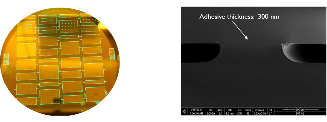
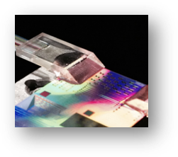
Allows to integrate microfluidic functionalities on top of Si CMOS sensor technology with noble metal top surface finish by means of wafer-level glass microfluidics. These technology combinations are suited for the fabrication of chemical, bio-chemical and medical devices but could also be of potential interest for high power applications that need liquid cooling for thermal management.
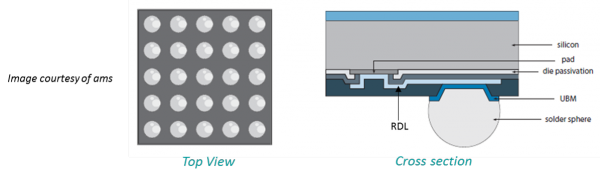
Building blocks
Si CMOS with noble metal sensor technology (add-on on X-FAB XH035)
Multi-layer glass wafer fabrication
Si-to-glass wafer-level bonding, key features:
– room temperature bonding for encapsulation of bio-materials
– ultra-thin selective adhesive transfer technology with excellent uniformity over large areas
– compatible with a wide range of materials, e.g. CTE
– compatible to wide range of P, T, pH
– abundance of Adhesives to suit
customer assay
– bio-compatibility assured
Design rules
The combination of these building blocks provides you an integrated solution of a Si CMOS sensor chip with micro-scaled glass microfluidic functionalities in direct contact with the Si surface. Additional routing layers inside the glass interposer chip may facilitate the further integration to macro-sized fluidic interfaces. Apart from the individual building block design rules, specific rules apply for the integration. Electrical access is provided through wire bonding and fluidic connection is realized through standard-sized fluidic access holes
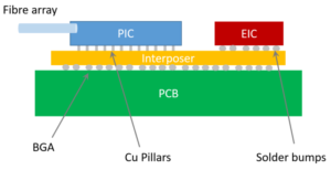
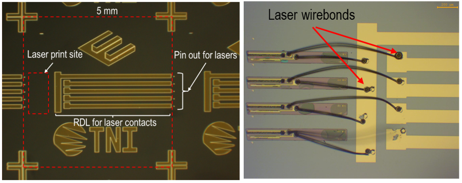
Contact

Riet Labie

e-mail: Riet.Labie@imec.be

Tel: +32 (0) 16 281 237


Fraunhofer and CMP provide access to this ams technology.

ams 0.35µm wafer-level bumping
Technology characteristics
Solder bumping consists in manufacturing metal spheres acting as interconnections for flip-chip. Those spheres are composed of a Sn/Ag/Cu alloy (SAC). Before the sphere can be deposited, the deposition of an Under Bump Metalization (UBM) layer is required. This option, available on ams 0.35 & 0.18 runs only, is operated at wafer-level within ams cleanroom after CMOS process. It allows the deposition of an array of solder balls at wafer-level, with an I/O pitch compatible with traditional printed circuit board (PCB) assembly processes. For mechanical reasons solder balls are usually evenly distributed over the whole chip surface and electrically connected to the IC‘s CMOS pads by means of a redistribution layer (RDL) included in the option.
Application area
Single die flip-chip packaging
Design Kit version
Option supported by ams hitkit 4.10 ISR15, through an add-on