
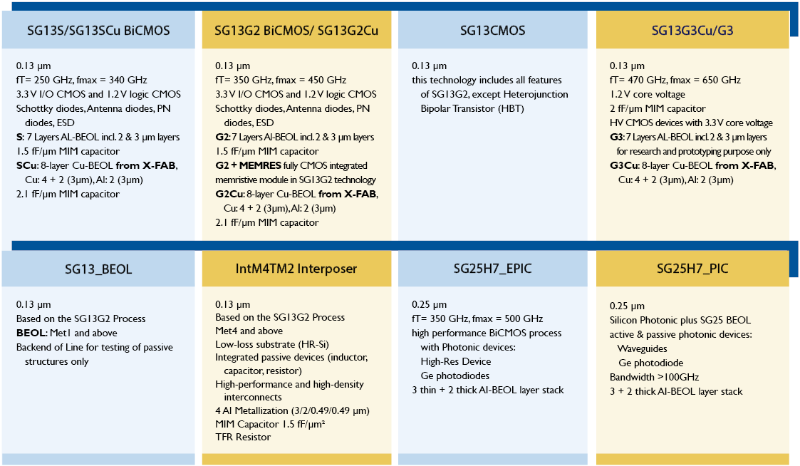
IHP offers standard 0.13 and 0.25 μm CMOS processes which provide NMOS, PMOS, isolated NMOS and passive components such as poly resistors and MIM capacitors. In addition to the standard CMOS processes different front-end-of-line options are offered.
0.25 μm CMOS process is a monolithic photonic BiCMOS technology combining 0.25 µm CMOS, high-performance npn HBTs, and full photonic device set for C/O-band with the standard Al-BEOL backend.
The BEOL backend for 0.13 μm process offers 5 thin and 2 thick metal layers (TM1: 2 μm TM2: 3 μm).
Together with a high dielectric stack this enables increased performance of the passive RF components.
Besides the Al-BEOL stack, IHP also offers the CU-BEOL stack. Using processes with Cu-Layers the following passive components can be improved compared with Al-BEOL:
SG13S | |
|---|---|
Technology characteristics | Met. layer(s): 7 5 thin metal layers, 2 thick metal layers BiPolar, CMOS devices MIM Cap, HRES, additional MEMRES module Available I/O: I/O digital cell library Standard cells database supports digital (front-end, backend and mixed-signal OA) design flow Temp. range: -40° C. / +125° C Thin gate oxide for the 1.2 V and a thick oxide for a 3.3 V supply voltage |
Special features | High performance RF technology |
Application area | wireless and broadband communications |
Frontend Backend tools
| Cadence 6.1.8, ADS, AWR, TexEDA |
Verification tools
| PVS (Cadence)/Calibre (Siemens)
|
Parasitic extraction tools | ORC (Cadence) |
Place route tools | Innovus (Cadence)
|
Libraries | Analog/ Standard Cell and IO digital libraries |
Turnaround time | 6 months
|
SG13G2 | |
|---|---|
Technology characteristics | Met. layer(s): 7 5 thin metal layers, 2 thick metal layers BiPolar, CMOS devices MIM Cap, HRES Available I/O: I/O digital cell library Standard cells database supports digital (front-end, backend and mixed-signal OA) design flows Temp. range: -40° C. / +125° C Thin gate oxide for the 1.2 V and a thick oxide for a 3.3 V supply voltage |
Special features | Very high-performance RF technology |
Application area | wireless and broadband communications |
Frontend Backend tools
| Cadence 6.1.8, ADS, AWR, TexEDA |
Verification tools
| PVS (Cadence)/Calibre (Siemens)
|
Parasitic extraction tools | ORC (Cadence) |
Place route tools | Innovus (Cadence)
|
Libraries | Analog/ Standard Cell and IO digital libraries |
Turnaround time | 6 months
|
SG13SCU-BEOL | |
|---|---|
Technology characteristics | Met. layer(s): 8 4 thin metal layers (Cu) 2 thick metal layers (Cu) 1 thin aluminium layer for MIM 1 thick aluminium layer for bondpad BiPolar, CMOS devices MIM Cap, HRES Available I/O: I/O digital cell library Standard cells database supports digital (front-end, backend and mixed-signal OA) design flow Temp. range: -40° C. / +125° C Thin gate oxide for the 1.2 V and a thick oxide for a 3.3 V supply voltage |
Special features | RF technology with the high performance, Improvement of passive components |
Application area | wireless and broadband communications |
Frontend Backend tools
| Cadence 6.1.8, ADS |
Verification tools
| PVS (Cadence)/Calibre (Siemens)
|
Parasitic extraction tools | ORC (Cadence) |
Place route tools | Innovus (Cadence)
|
Libraries | Analog/ Standard Cell and IO digital libraries |
Turnaround time | 6 months
|
SG13G2CU-BEOL | |
|---|---|
Technology characteristics | Met. layer(s): 8 4 thin metal layers (Cu) 2 thick metal layers (Cu) 1 thin aluminium layer for MIM 1 thick aluminium layer for bondpad BiPolar, CMOS devices MIM Cap, HRES Available I/O: I/O digital cell library Standard cells database supports digital (front-end, backend and mixed-signal OA) design flow Temp. range: -40° C. / +125° C Thin gate oxide for the 1.2 V and a thick oxide for a 3.3 V supply voltage |
Special features | RF technology with very high performance, Improvement of passive components |
Application area | wireless and broadband communications |
Frontend Backend tools
| Cadence 6.1.8, ADS |
Verification tools
| PVS (Cadence)/Calibre (Siemens)
|
Parasitic extraction tools | ORC (Cadence) |
Place route tools | Innovus (Cadence)
|
Libraries | Analog/ Standard Cell and IO digital libraries |
Turnaround time | 6 months
|
SG13G3CU-BEOL | |
|---|---|
Technology characteristics | Met. layer(s): 8 4 thin metal layers (Cu) 2 thick metal layers (Cu) 1 thin aluminium layer for MIM 1 thick aluminium layer for bondpad BiPolar, CMOS devices MIM Cap, HRES Standard cells database supports digital (front-end, backend and mixed-signal OA) design flow Temp. range: -40° C. / +125° C Thin gate oxide for the 1.2 V and a thick oxide for a 3.3 V supply voltage |
Special features | RF technology with the highest bipolar performance, Improvement of passive components |
Application area | wireless and broadband communications |
Frontend Backend tools
| Cadence 6.1.8, ADS |
Verification tools
| PVS (Cadence)/Calibre (Siemens)
|
Parasitic extraction tools | ORC (Cadence) |
Place route tools | Innovus (Cadence)
|
Libraries | Analog/digital |
Turnaround time | 7 months
|
SG13G3 | |
|---|---|
Technology characteristics | Met. layer(s): 7 5 thin metal layers, 2 thick metal layers BiPolar, CMOS devices MIM Cap, poly silicon resistors Available I/O: I/O digital cell library Standard cells database supports digital (front-end, backend and mixed-signal OA) design flows Temp. range: -40° C. / +125° C Thin gate oxide for the 1.2 V and a thick oxide for a 3.3 V supply voltage |
Special features | BiCMOS technology with very high bipolar performance |
Application area | wireless and broadband communications |
Frontend Backend tools
| Cadence 6.1.8, ADS |
Verification tools
| PVS (Cadence)/Calibre(Siemens) |
Parasitic extraction tools | QRC (Cadence) |
Place route tools | Innovus (Cadence)
|
Libraries | Analog/Standard Cell and IO digital libraries |
Turnaround time | 7 months
|
SG25H7_EPIC | |
|---|---|
Technology characteristics | Met. layer(s): 5 3 thin metal layers, 2 thick metal layers BiPolar, CMOS devices, high-responsivity Ge photodiodes MIM Cap, HRES, passive photonic components Available I/O: I/O digital cell library Standard cells database supports digital (front-end, backend and mixed-signal OA) design flow Temp. range: -40° C. / +125° C Thin gate oxide for the 1.2 V and a thick oxide for a 3.3 V supply voltage https://europractice-ic.com/technologies/photonics/ihp/ |
Special features | Monolithic photonic BiCMOS technology combining RF-MOS, high-performance HBTs and full photonic device set for C/O-band. Enabling the fabrication of electronic-photonic integrated circuit. High RF passive component performance |
Application area | Optical communication systems, Broadband communications |
Frontend Backend tools
| Cadence 6.1.8, ADS, IPKISS, Tanner,TexEDA |
Verification tools
| PVS (Cadence)/Calibre(Siemens) |
Parasitic extraction tools | QRC (Cadence)/XRC |
Place route tools | Innovus (Cadence)
|
Libraries | Analog/ digital 3.3V I/O and standard library |
Turnaround time | 9 months
|
Graphene | |
|---|---|
Technology characteristics | IHP focuses on the development of graphene photonic integrated circuits (PIC) in a 200 mm pilot line. More details can be found here: https://europractice-ic.com/technologies/graphene/ihp-graphene/ https://graphene-flagship.eu/industrialisation/pilot-line/2d-pl-support-programme |
Special features | Fabrication of Graphene photonic devices in 200 mm BiCMOS pilot line with tailored processes. Graphene-based PICs combined with embedded SiN waveguides. |
Application area | Testing of diverse components for advanced high-speed communication, optical computing, etc. systems. Creation of ultra-thin and lightweight components, enabling the development of faster and more efficient electronic devices. Application fields in healthcare, environmental monitoring, and consumer electronics |
Design tools
| Klayout, TeXeda |
Verification tools
| Klayout, TeXeda DRC |
Libraries | Preliminary device libraries including waveguide, grating coupler, modulator performances |
Turnaround time | 4 – 5 months |