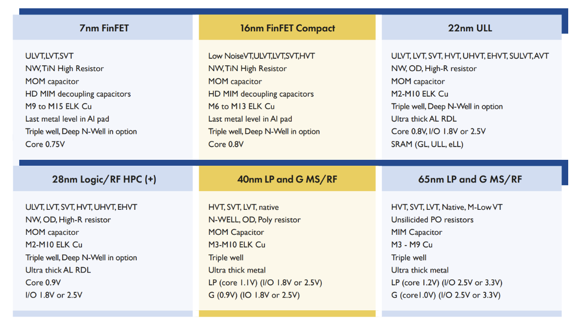
This is an overview of the most popular TSMC technologies. You can find more technology flavours in the ‘Details’ section below.
From now on, customers can also get access to the backend views of standard cell libraries, as long as there is a firm tape out plan. To request the access, please complete this form.
Your request will be reviewed by TSMC. We would like to warn you that the review procedure can take up to 3 months due to high number of applications.
It is a popular and well supported node.
65nm CMOS Logic or MS/RF, General purpose | |
|---|---|
Technology characteristics | Shrink technology: NO Core voltage: 1.0V I/O voltage: 2.5V (1.8V underdrive, 3.3V overdrive) Shallow Trench Isolation (STI) Wells: Retrograde twin well for low well sheet resistance and better latch-up behavior. Optional Deep N-Well <100> P- substrate wafer. Substrate resistivity 8-12ohm-cm Dual Gate Oxide (1 for core, 1 for IO) Vt options: lvt, svt, hvt, native Temperature range: -40C to 125C # of metals: 3 to 9 Cu + alrdl Interconnect dielectric: LK Top metal: 5KA, 9KA, 12.5KA, 34KA CMP on STI, contact, metals, vias and passivation MoM MiM density: 1fF/µm2, 1.5fF/µm2 or 2fF/µm2, mutually exclusive Passivation: dual layers |
Options that need special attention
| OTP/MTP SRAM Cell |
Wafer size | 12 inch
|
Deliverables | # of dies (no wafer!): 100 dies / wafer
|
Design tools | PDK: Cadence CDBA and OA, TSMC iPDK, Mentor
|
Simulation tools | HSPICE, Eldo, Spectre
|
Verification tools DRC | Cadence, Siemens EDA, Synopsys, Magma, TSMC iDRC
|
Verification tools LVS
| Cadence, Siemens EDA, Synopsys, Magma
|
Parasitic extraction tools
| Cadence, Siemens EDA, Synopsys
|
P&R tools
| Cadence, Siemens EDA, Synopsys
|
Foundry IP
| 12-track / 10-track / 9-track core cell libraries, multi-vt, coarse grain 1.0V/2.5V staggered (fail-safe digital, 5V input tolerant digital, hybrid small footprint digital/analog and regular analog) I/O library SRAM compilers from 3rd party |
MPW block size
| 12 mm2
|
Mini@sic characteristics
| Not Supported |
It is a popular and well supported node.
65nm CMOS Logic or MS/RF, Low Power | |
|---|---|
Technology characteristics | Shrink technology: NO Core voltage: 1.2V I/O voltage: 2.5V (1.8V underdrive, 3.3V overdrive) Shallow Trench Isolation (STI) Wells: Retrograde twin well for low well sheet resistance and better latch-up behavior. Optional Deep N-Well <100> P- substrate wafer. Substrate resistivity 8-12ohm-cm Dual Gate Oxide (1 for core, 1 for IO) Vt options: lvt, svt, hvt, mLowvt, native Temperature range: -40C to 125C # of metals: 3 to 9 Cu + alrdl Interconnect dielectric: LK Top metal: 5KA, 9KA, 12.5KA, 34KA CMP on STI, contact, metals, vias and passivation MoM MiM density: 1fF/µm2, 1.5fF/µm2 or 2fF/µm2, mutually exclusive Passivation: dual layers |
Options that need special attention
| OTP/MTP SRAM Cell |
Wafer size | 12 inch
|
Deliverables | # of dies (no wafer!): 100 dies / wafer
|
Design tools | PDK: Cadence CDBA and OA, TSMC iPDK, Mentor
|
Simulation tools | HSPICE, Eldo, Spectre
|
Verification tools DRC | Cadence, Siemens EDA, Synopsys, Magma, TSMC iDRC
|
Verification tools LVS
| Cadence, Siemens EDA, Synopsys, Magma
|
Parasitic extraction tools
| Cadence, Siemens EDA, Synopsys
|
P&R tools
| Cadence, Siemens EDA, Synopsys
|
Foundry IP
| 12-track / 10-track / 9-track / 7-track core cell libraries, multi-vt, coarse grain 1.2V/2.5V staggered (fail-safe digital, 5V input tolerant digital, hybrid small footprint digital/analog and regular analog) I/O library 1.2V/2.5V linear (digital, hybrid small footprint digital/analog and regular analog) I/O library SRAM compilers |
MPW block size
| 12 mm2
|
Mini@sic characteristics
| |
Well supported advanced node, 40G = 45GS.
40nm CMOS Logic or MS/RF, General Purpose | |
|---|---|
Technology characteristics | Shrink technology: YES Core voltage: 0.9V I/O voltage: 2.5V (1.8V underdrive, 3.3V overdrive) or true 1.8V Shallow Trench Isolation (STI) Wells: Retrograde twin well for low well sheet resistance and better latch-up behavior. Optional Deep N-Well <110> P- substrate wafer. Substrate resistivity 8-12ohm-cm Dual Gate Oxide (1 for core, 1 for IO) Vt options: lvt, svt, hvt, native Temperature range: -40C to 125C # of metals: 3 to 10 Cu + alrdl Interconnect dielectric: ELK Top metal: 3.1KA, 9KA, 12.5KA, 34KA CMP on STI, contact, metals, vias and passivation MoM Passivation: dual layers |
Options that need special attention
| OTP/MTP SRAM Cell |
Wafer size | 12 inch
|
Deliverables | # of dies (no wafer!): 100 dies / wafer
|
Design tools | PDK: Cadence CDBA and OA, TSMC iPDK
|
Simulation tools | HSPICE, Eldo, Spectre
|
Verification tools DRC | Cadence, Siemens EDA, Synopsys, Magma, TSMC iDRC
|
Verification tools LVS
| Cadence, Siemens EDA, Synopsys, Magma, TSMC iLVS
|
Parasitic extraction tools
| Cadence, Siemens EDA, Synopsys
|
P&R tools
| Cadence, Siemens EDA, Synopsys
|
Foundry IP
| 12-track / 9-track core cell libraries, multi-vt, coarse grain 0.9V/1.8V staggered (fail-safe digital, 5V input tolerant digital and regular analog) I/O library 0.9V/2.5V staggered (fail-safe digital, 5V input tolerant digital and regular analog) I/O library SRAM compilers |
MPW block size
| 9 mm2
|
Mini@sic characteristics
| Not supported
|
It is a well supported advanced node.
40nm CMOS Logic or MS/RF, Low Power | |
|---|---|
Technology characteristics | Shrink technology: YES (90% linear shrink) Core voltage: 1.1V I/O voltage: 2.5V (1.8V underdrive, 3.3V overdrive) Shallow Trench Isolation (STI) Wells: Retrograde twin well for low well sheet resistance and better latch-up behavior. Optional Deep N-Well <110> P- substrate wafer. Substrate resistivity 8-12ohm-cm Dual Gate Oxide (1 for core, 1 for IO) Vt options: lvt, svt, hvt, native Temperature range: -40C to 125C # of metals: 3 to 10 Cu + alrdl Interconnect dielectric: ELK Top metal: 3.1KA, 9KA, 12.5KA, 34KA CMP on STI, contact, metals, vias and passivation MoM Passivation: dual layers |
Options that need special attention
| OTP/MTP SRAM Cell |
Wafer size | 12 inch
|
Deliverables | # of dies (no wafer!): 100 dies / wafer
|
Design tools | PDK: Cadence CDBA and OA, TSMC iPDK, Mentor
|
Simulation tools | HSPICE, Eldo, Spectre
|
Verification tools DRC | Cadence, Siemens EDA, Synopsys, Magma, TSMC iDRC
|
Verification tools LVS
| Cadence, Siemens EDA, Synopsys, Magma, TSMC iLVS
|
Parasitic extraction tools
| Cadence, Siemens EDA, Synopsys
|
P&R tools
| Cadence, Siemens EDA, Synopsys
|
Foundry IP
| 12-track / 9-track core cell libraries, multi-vt, coarse grain 1.1V/2.5V staggered (fail-safe digital, 5V input tolerant digital, hybrid small footprint digital/analog and regular analog) I/O library SRAM compilers |
MPW block size
| 9 mm2
|
Mini@sic characteristics
| |
The TSMC 28nm technology is the most performant planar mainstream solution that evolved through the years due to constant enhancements in the manufacturing process. It supports a wide range of applications, including CPUs, GPUs, high-speed networking chips, smart phones, APs, tablets, home entertainment, consumer electronics, automotive and IoT.
The 28nm RF (28HPC+ RF) technology also provides support for 110GHz mmWave and for 5G mmWave RF.
28nm CMOS HPC+ Logic, RF | |
|---|---|
Technology characteristics | Shrink technology: YES Core voltage: 0.9V I/O voltage: – MPW (1.8V or 2.5V), – mini@sic (1.8V only) Shallow Trench Isolation (STI) Wells: Retrograde twin well for low well sheet resistance and better latch-up behavior. Triple well, Deep N-Well in option Dual Gate Oxide Vt options (only 4 out of 7): ulvt, lvt, hvt, uhvt, ehvt, sram, sram_ull 1.8V I/O based 5V HVMOS: Not offered for RF HPC+ flavor HighRes resistors Temperature range: -40C to 125C # of metals: 5 to 10 Cu + ALRDL Interconnect dielectric: ELK Top metal: Up to 35kA (please check with eptsmc@imec.be first) CMP on STI, contact, via and passivation MoM capacitor Passivation: dual layers |
Options that need special attention
| SRAM Cell (GL, ULL) Vt’s: maximum of 4 VT types in one design. |
Wafer size | 12 inch
|
Deliverables | 100 dies, no wafer
|
Design tools | PDK: TSMC iPDK
|
Simulation tools | HSPICE, Eldo, Spectre
|
Verification tools DRC | Cadence, Siemens EDA, Synopsys
|
Verification tools LVS
| Cadence, Siemens EDA, Synopsys
|
Parasitic extraction tools
| Cadence, Siemens EDA, Synopsys
|
P&R tools
| Cadence, Siemens EDA, Synopsys
|
Foundry IP
| 12-track / 9-track / 7-track core cell libraries, multi-vt’s 0.9V/1.8V hybrid staggered (fail-safe digital and regular analog) I/O library SRAM compilers by TSMC , ARM, Synopsys |
MPW block size
| 6mm² (on silicon)
|
Mini@sic characteristics
| |
The TSMC 28nm technology is the most performant planar mainstream solution that evolved through the years due to constant enhancements in the manufacturing process. It supports a wide range of applications, including CPUs, GPUs, high-speed networking chips, smart phones, APs, tablets, home entertainment, consumer electronics, automotive and IoT.
28nm CMOS HPC Logic, RF | |
|---|---|
Technology characteristics | Shrink technology: YES Core voltage: 0.9V I/O voltage: MPW (1.8V or 2.5V) Shallow Trench Isolation (STI) Wells: Retrograde twin well for low well sheet resistance and better latch-up behavior. Triple well, Deep N-Well in option Dual Gate Oxide Vt options (only 4 out of 7): ulvt, lvt, hvt, uhvt, ehvt, sram, sram_ull 1.8V I/O based 5V HVMOS HighRes resistors Temperature range: -40C to 125C # of metals: 5 to 10 Cu + ALRDL Interconnect dielectric: ELK Top metal: Up to 35kA (please check with eptsmc@imec.be first) CMP on STI, contact, via and passivation MoM capacitor Passivation: dual layers |
Options that need special attention
| SRAM Cell (GL, LL) Vt’s: maximum of 4 VT types in one design. |
Wafer size | 12 inch
|
Deliverables | 100 dies, no wafer
|
Design tools | PDK: TSMC iPDK
|
Simulation tools | HSPICE, Eldo, Spectre
|
Verification tools DRC | Cadence, Siemens EDA, Synopsys
|
Verification tools LVS
| Cadence, Siemens EDA, Synopsys
|
Parasitic extraction tools
| Cadence, Siemens EDA, Synopsys
|
P&R tools
| Cadence, Siemens EDA, Synopsys
|
Foundry IP
| 12-track / 9-track / 7-track core cell libraries, multi-vt’s 0.9V/1.8V hybrid staggered (fail-safe digital and regular analog) I/O library SRAM compilers by TSMC , ARM, Synopsys |
MPW block size
| 6mm² (on silicon)
|
Mini@sic characteristics
| Not supported |
TSMC’s 22nm technology is developed based on its 28nm process. Europractice supports the Ultra Low Leakage flavor of the process: 22ULL. The technology is TSMC’s most advanced planar node. Compared to the 28nm high-performance compact (28HPC) technology, it provides a 10% area reduction with more than 10% speed gain or 20% power reduction. It is suitable for applications including mobile devices, automotive electronics, IoT and consumer products. Additionally, TSMC’s 22nm ULL RF technology adds key mmWave mobile communication devices.
22nm CMOS ULP and ULL | |
|---|---|
Technology characteristics | Shrink technology: YES (85.5% linear shrink from 32nm) Core voltage: 0.8V I/O voltage: 1.8V or 2.5V Shallow Trench Isolation (STI) Wells: Retrograde twin well for low well sheet resistance and better latch-up behavior Triple well, Deep N-Well in option Dual Gate Oxide Vt options: – ULP: UHVt, HVt, SVt, LVt, ULVt, Native – ULL: UHVt, HVt, SVt, LVt, ULVt, EHVt, Native SRAM: – ULP: GL SRAM – ULL: GL SRAM, ULL SRAM, ELL SRAM High-R and unsilicided OD resistors NW resistors: NW resistor within OD and NW resistor under STI Temperature range: -40C to 125C junction temperature # of metals: 3 to 10 Cu + AlRDL Top metal: Up to 35KA (please check with eptsmc@imec.be) HVMOS: – I/O 1.8V based HVMOS in ULL/ULP – I/O 2.5V based HVMOS in ULL only CMP on STI, contact, metals, vias, passivation |
Wafer size | 12 inch
|
Deliverables | 100 dies, no wafer
|
Design tools | PDK: TSMC iPDK
|
Verification tools DRC | Cadence, Siemens EDA, Synopsys
|
Verification tools LVS
| Cadence, Siemens EDA, Synopsys
|
Parasitic extraction tools
| Cadence, Siemens EDA, Synopsys
|
P&R tools
| Cadence, Synopsys
|
I/O | 0.8V/1.8V or 0.8V/2.5V. 2.5V overdrive to 3.3V 2.5V underdrive to 1.8V 1.8V underdrive to 1.5V 1.8V underdrive to 1.2V |
SRAM | ULP: SRAM compilers by TSMC ULL: SRAM compilers by ARM |
MPW block size
| 6 mm² (on silicon)
|
Mini@sic characteristics
| Not supported
|
Europractice offers a flagship technology TSMC 16nm CMOS logic or RF FinFET Compact 0.8V/1.8V. It provides superior performance and power consumption advantage for next generation high-end mobile computing, network communication, consumer and automotive electronic applications.
16nm CMOS logic FinFET Compact | |
|---|---|
Technology characteristics | Shrink technology: 2% shrink Core voltage: 0.8V I/O voltage: 1.8V Shallow Trench Isolation (STI) Triple well, Deep N-Well in option Dual gate oxide Vt options: hvt, svt, lvt, ulvt, low noise vt 5V HVMOS TiN High Resistor N+/P+ metal gate allows symmetrical design of NMOS and PMOS devices Temperature range: -40C to 125C # of metals: 6 to 13 Cu plus last metal level in Al pad Interconnect dielectric: ELK HD MiM capacitors Passivation: dual layers |
Wafer size | 12 inch
|
Deliverables | 100 dies, no wafer
|
Design tools | PDK: TSMC iPDK
|
Simulation tools | HSPICE, Eldo, Spectre
|
Verification tools DRC | Cadence, Siemens EDA, Synopsys
|
Verification tools LVS
| Cadence, Siemens EDA, Synopsys
|
Parasitic extraction tools
| Cadence, Siemens EDA, Synopsys
|
P&R tools
| Cadence, Siemens EDA, Synopsys
|
Foundry IP
| 9-track, 7.5-track body biased core cell libraries with gate lengths of 16, 20 and 24nm 0.8V/1.8V hybrid staggered I/O library SRAM compilers by TSMC, ARM_Artisan, ARM ltd, GUC, Synopsys |
MPW block size
| 4 mm²
|
Mini@sic characteristics
| |
TSMC 7nm FinFET offers industry-leading power and performance for a broad array of applications, ranging from high-to-mid end mobile,
consumer applications, AI, networking, 5G infrastructure, GPU, and high-performance computing.
Since it is classified as a leading node technology, access to it is subject to review and approval by TSMC.
7nm CMOS logic FinFET Compact | |
|---|---|
Technology characteristics | Shrink technology: NO Core voltage: 0.75V I/O voltage: 1.8V Shallow Trench Isolation (STI) Triple well, Deep N-Well in option Dual gate oxide Vt options: svt, lvt, ulvt NW, TiN High Resistor N+/P+ metal gate allows symmetrical design of NMOS and PMOS devices Temperature range: -40C to 125C # of metals: 9 to 15 Cu plus last metal level in Al pad Interconnect dielectric: ELK MOM capacitors HD MiM capacitors for decoupling Passivation: dual layers |
Wafer size | 12 inch
|
Deliverables | 100 dies, no wafer
|
Design tools | PDK: TSMC iPDK
|
Simulation tools | HSPICE, Eldo, Spectre
|
Verification tools DRC | Cadence, Siemens EDA, Synopsys
|
Verification tools LVS
| Cadence, Siemens EDA, Synopsys
|
Parasitic extraction tools
| Cadence, Siemens EDA, Synopsys
|
P&R tools
| Cadence, Siemens EDA, Synopsys
|
Foundry IP
| Cell height 240nm or 300nm, body biased PODE core cell libraries with gate lengths of 8 and 11nm 0.75V/1.8V, general purpose I/O library in combination with solder bump or Cu-pillar (no wirebond) SRAM compilers |
MPW block size
| 2 mm²
|
Mini@sic characteristics
| Not supported
|
Discover TSMC metal stacks options and mini@sic options available through Europractice: