Europractice customers can obtain access to the following X-FAB technologies.
X-FAB Technologies | |
|---|---|
NEW XT011 | XT011 is X-FAB’s next generation BCD-on-SOI technology. It combines the benefit of SOI wafers with Deep Trench Isolation (DTI) and those of a state-of-the-art 110 nm process. It offers more than twice the standard cell library density compared to XT018.
XT011 features multiple high voltage options and a range of automotive Grade-0 non-volatile memory options. The XT011 platform is specifically designed for a next generation automotive, industrial, and medical applications operating in the temperature range of -40°C to 175°C. |
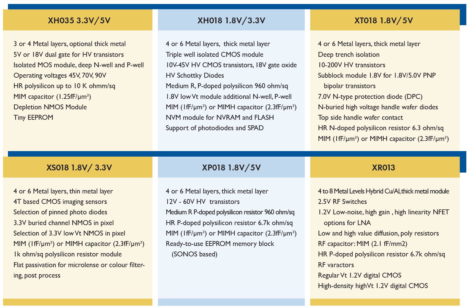
XH035
| The XH035 series is X-FAB’s 0.35 micrometre Modular Mixed-Signal Technology.
Main target applications are standard cell, semi-custom and full custom designs for industrial, automotive and telecommunication products. Based on a single poly triple metal 0.35μm drawn gate length process for digital applications, it features core and process modules such as low Vt, low leakage, embedded non-volatile memory and high voltage options, as well as standard or thick fourth layer of metal, double poly and MIM capacitors and high resistance polysilicon. MOS and bipolar transistors are also available. World class low noise p-mos and n-mos transistors make this technology the first choice for applications requiring very low noise and high signal-to-noise ratios. DMOS transistors are available for multiple operating voltages up to 100V. The 45V DMOS transistors come with a 45 percent lower on-resistance which can reduce the chip area by up to 40 percent, resulting in significant cost savings. The 3.3 V CMOS cores are compatible in design rules and transistor performance with state-of-the-art 0.35μm CMOS processes. |
XH035_noble metal
| An add-on option is available to XH035 technology that provides a noble metal finish layer on top of the CMOS passivation. This additional finish can be either Au- or Pt-terminated and is usable as electrode material for sensor applications. It is connected to the standard top (Al) metal by the use of W-through passivation vias. This option is available for MLM services. Specific design rules and requirements apply. |
XH018
| The XH018 series is X-FAB’s 0.18 micron Modular Mixed Signal HV CMOS Technology. Based upon the industrial standard single poly with up to six metal layers 0.18-micron drawn gate length Nwell process. It is the industry’s first and only 0.18 micrometer technology to integrate high temperature (HT), high voltage (HV) and non-volatile memory (NVM) all in a single platform. It is ideal for SoC applications in the automotive market such as control devices inside combustion engine compartments or electric engine housings with temperature range up to 175ºC, as well as embedded high-voltage applications in the communications, consumer and industrial market. |
XT018
| The XT018 series is X-FAB’s 0.18-micron Modular High-voltage SOI CMOS Technology. It combines the benefit of SOI wafers with Deep Trench Isolation (DTI) and those of a state-of-the-art six metal layers 0.18-micron process. High voltage support up to 200V combined with range of Non-Volatile-Memory options. The XT018 platform is specifically designed for a next generation automotive, industrial and medical applications operating in the temperature range of -40 to 175 °C. The platform is ideal for consumer, medical, telecommunication infrastructure and industrial applications that need bidirectional isolation, such as PoE applications, ultrasound transmitter drivers, piezo actuators and capacitive-driven micromechanics. |
XS018
| XS018 is X-FAB’s specialized process for fast image sensors. The optional available modules for 4 transistor cells, pinned photo diodes and the stitching capabilities make this technology ideal for large image sensor applications needing high frame rates as used for instance for medical and scientific X-ray cameras. The 3.3V core module allows a low mask count designs. The industrial standard single poly with up to six metal layers 0.18-micron drawn gate length N-well process can also be used for low power SOC application in the automotive, industrial and medical markets. |
XP018
| The XP018 series is X-FAB’s 0.18 micron Modular CMOS High Performance Analog Mixed-Signal Technology. Based upon the industrial standard single poly with up to six metal layers 0.18-micron drawn gate length N-well process, integrated with high voltage and Non-Volatile-Memory modules, the platform is engineered for applications needing an integrated solution and cost efficient process for high performance ICs. Targeted applications are switching applications, lightings, display, etc; operating in temperature range of -40 to 175 °C. |
XR013
| The XR013 technology is a RF SOI (CMOS) 0.13µm generation designed to serve RF applications. High-resistive ‘trap-rich’ SOI substrate (>3 kΩ-cm). Low Ron*Coff switch NMOS transistor with minimum L = 0.22µm. Vertical parallel plate (VPP) capacitor and Metal-Insulator-Metal (MIM) capacitor. |
XMB10 MEMS
| Explore the XMB10 MEMS technology details. |
XT011 is X-FAB’s next generation BCD-on-SOI technology. It combines the benefit of SOI wafers with Deep Trench Isolation (DTI) and those of a state-of-the-art 110 nm process. It offers more than twice the standard cell library density compared to XT018.
XT011 features multiple high voltage options and a range of automotive Grade-0 non-volatile memory options. The XT011 platform is specifically designed for a next generation automotive, industrial, and medical applications operating in the temperature range of -40°C to 175°C.
XT011: Next generation BCD-on-SOI technology | |
|---|---|
Key Features | • Fully modular 110nm SOI process based on low mask count 5V Single Gate core module • Up to eight metal layers with different thick metal options • Deep Trench Isolation • Up to 175ºC operating temperature supporting AEC-Q100 Grade 0 • Unique integration of digital, analog, HV, NVM and SOI in a single process • High-reliability automotive NVM solutions including Flash • 12V – 60V HV CMOS transistors • Excellent specific Ron HV N-channel device performance • Metal Fringe capacitors |
Wafer size | 200mm
|
Deliverables | number of dies: MPW – 50 standard dies |
Design tools | Cadence, Mentor, Synopsys and Tanner |
Simulation tools | Spectre (Cadence) |
Verification tools DRC | PVS (Cadence), Calibre (Siemens EDA) |
Verification tools LVS
| PVS (Cadence), Calibre (Siemens EDA) |
Parasitic extraction tools
| QRC (Cadence) |
P&R tools
| Cadence
|
Foundry IP
| N/A |
MPW block size
| minimum 10 mm2, flexible aspect ratio
|
Mini@sic characteristics
| NOT Supported |
Turnaround time | Typical leadtime: ~23 weeks from Tapeout date to samples out |
The XH035 series is X-FAB’s 0.35 micrometre Modular Mixed-Signal Technology. Main target applications are anolog, high-voltage and sensor/actuator designs for industrial, automotive and medical products. Based on a single poly triple metal 0.35μm drawn gate length process for digital applications, it features core and process modules such as low Vt, low leakage, embedded non-volatile memory and high voltage options, as well as standard or thick fourth layer of metal, double poly and MIM capacitors and high resistance polysilicon. MOS and bipolar transistors are also available. World class low noise p-mos and n-mos transistors make this technology the first choice for applications requiring very low noise and high signal-to-noise ratios.
DMOS transistors are available for multiple operating voltages up to 100V. The 45V DMOS transistors come with a 45 percent lower on-resistance which can reduce the chip area by up to 40 percent, resulting in significant cost savings.
The 3.3 V CMOS cores are compatible in design rules and transistor performance with state-of-the-art 0.35μm CMOS processes.
XH035: Modular Mixed-Signal Technology with HV Extensions | |
|---|---|
Key Features | • Fully modular 350 nm EPI process based on 3.3 V ultra-low noise core module • Alternative 5 V core module or 3.3 V / 5 V dual gate • Best-in-class ultra-low noise 3.3 V PMOS • Up to four metal layers with thick metal options • Up to 125 ºC operating temperature supporting AEC-Q100 grade 1 • Unique integration of digital, analog, HV and NVM in a single process • High-reliability automotive NVM solutions including EEPROM • Optical window etching and Anti Reflecting Coating for high sensitive photodiodes • 10 V – 100 V HV CMOS transistors with 3.3 V, 5 V or 18 V Gate Oxide • High gain BJTs • HV Schottky diodes • Standard single, double MIM, Poly and metal fringe capacitors |
Wafer size | 200mm
|
Deliverables | number of dies: MPW – 50 standard dies |
Design tools | Cadence |
Simulation tools | Cadence |
Verification tools DRC | PVS (Cadence), Calibre (Siemens EDA) |
Verification tools LVS
| PVS (Cadence), Calibre (Siemens EDA) |
Parasitic extraction tools
| QRC (Cadence) |
P&R tools
| Cadence
|
Foundry IP
| 3.3V analog IP cells I/O cells RAM/ROM Memory Compilers |
MPW block size
| minimum 10 mm2, flexible aspect ratio
|
Mini@sic characteristics
| NOT Supported |
Turnaround time | Typical leadtime: ~19 weeks from Tapeout date to samples out |
The XH018 series is X-FAB’s 0.18 micron Modular Mixed Signal HV CMOS Technology.
Based upon the industrial standard single poly with up to six metal layers 0.18-micron drawn gate length Nwell process.
It is the industry’s first and only 0.18 micrometer technology to integrate high temperature (HT), high voltage (HV) and non-volatile memory (NVM) all in a single platform.
It is ideal for SoC applications in the automotive market such as control devices inside combustion engine compartments or electric engine housings with temperature range up to 175ºC, as well as embedded high-voltage applications in the communications, consumer and industrial market.
XH018: Modular Mixed-Signal HV CMOS Technology | |
|---|---|
Key Features | • Fully modular 180 nm EPI process based on 1.8 V / 3.3 V dual gate core module • Up to six metal layers with different thick metal options • Up to 175ºC operating temperature supporting AEC-Q100 grade 0 • Unique integration of digital, analog, HV and NVM in a single process • High-reliability automotive NVM solutions including embedded Flash, NVRAM and OTP • Optional ultra-low-noise 1.8 V and 3.3 V CMOS • Fully characterized photodiodes and APD/SPAD • 10 V to 45 V high-voltage CMOS transistors with 18 V gate oxide • High gain BJTs • HV Schottky diodes • Standard and high capacitance single, double, triple MIM and metal fringe capacitors • Multiple 1.8 V and 3.3 V libraries available to enable complex designs |
Wafer size | 200mm
|
Deliverables | number of dies: MPW – 50 standard dies mini@sic – 50 standard dies |
Design tools | Cadence, Siemens EDA, Synopsys |
Simulation tools | Cadence, Siemens EDA, Synopsys |
Verification tools DRC | PVS (Cadence), Calibre (Siemens EDA) |
Verification tools LVS
| PVS (Cadence), Calibre (Siemens EDA) |
Parasitic extraction tools
| QRC (Cadence) |
P&R tools
| Cadence
|
Foundry IP
| 1.8V and 3.3V analog IP cells I/O cells RAM & ROM Memory Compliler |
MPW block size
| minimum 10 mm2, flexible aspect ratio |
Mini@sic characteristics
| Supported Block size: 1520µm x 1520µm Metal stack: MET1-MET2-MET3-MET4-METMID-METTHK Capacitor: MIM |
Turnaround time | Typical leadtime: ~23 weeks from Tapeout date to samples out |
The XT018 series is X-FAB’s 0.18-micron Modular High-voltage SOI CMOS Technology.
It combines the benefit of SOI wafers with Deep Trench Isolation (DTI) and those of a state-of-the-art six metal layers 0.18-micron process.
High voltage support up to 375V combined with range of Non-Volatile-Memory options.
The XT018 platform is specifically designed for a next generation automotive, industrial and medical applications operating in the temperature range of -40 to 175 °C. The platform is ideal for consumer, medical, telecommunication infrastructure and industrial applications that need bidirectional isolation, such as PoE applications, ultrasound transmitter drivers, piezo actuators and capacitive-driven micromechanics.
XT018: Modular HV SOI CMOS Technology | |
|---|---|
Key Features | • Fully modular 180 nm SOI process based on low mask count 5 V Single Gate core module • Up to six metal layers with different thick metal options • Deep Trench Isolation and handle wafer contact • Up to 175 ºC operating temperature supporting AEC-Q100 Grade 0 • Unique integration of digital, analog, HV, NVM and SOI in a single process • High-reliability automotive NVM solutions including embedded Flash, EEPROM and OTP • 10 V to 375 V high-voltage CMOS transistors • Excellent specific Ron HV N-channel device performance • High gain BJTs • Very fast forward HV, Schottky and Zener diodes • Standard and high capacitance single, double, triple MIM and metal fringe capacitors • Silicon Frontline R3D support for metal optimization |
Wafer size | 200mm
|
Deliverables | number of dies: MPW – 50 standard dies mini@sic – 50 standard dies |
Design tools | Cadence, Siemens EDA, Synopsys |
Simulation tools | Cadence, Siemens EDA, Synopsys |
Verification tools DRC | PVS (Cadence), Calibre (Siemens EDA) |
Verification tools LVS
| PVS (Cadence), Calibre (Siemens EDA) |
Parasitic extraction tools
| QRC (Cadence) |
P&R tools
| Cadence
|
Foundry IP
| 1.8V and 5V analog IP cells I/O cells RAM & ROM Memory Compiler |
MPW block size
| minimum 10 mm2, flexible aspect ratio |
Mini@sic characteristics
| Supported Block size: 1520µm x 1520µm Metal stack: MET1-MET2-MET3-MET4-METMID-METTHK-BASICPV Capacitor: MIMH |
Turnaround time | Typical leadtime: ~30 weeks weeks from Tapeout date to samples out |
XS018 is X-FAB’s specialized process for fast image sensors.
The optional available modules for 4 transistor cells, pinned photo diodes and the stitching capabilities make this technology ideal for large image sensor applications needing high frame rates as used for instance for medical and scientific X-ray cameras.
The 3.3V core module allows a low mask count designs.
The industrial standard single poly with up to six metal layers 0.18-micron drawn gate length N-well process can also be used for low power SOC application in the automotive, industrial and medical markets.
XS018: Specialized Process for Fast Image Sensors | |
|---|---|
Key Features | • Fully modular 180nn EPI process based on low mask count 3.3V Single Gate core module • 3.3V/1.8V core process options • Up to six metal layers with different thick metal options • Thin top metal option • Pinned photodiode module with choice of 4 different pinning voltages • Low threshold voltage NMOS with choice of 5 different threshold voltages • Pixel reference designs from 3.6 to 200µm • Six different photodiodes supporting UV, ambient and NIR light • High value poly resistors • Standard and High capacitance single, double, triple MIM and Metal Fringe capacitors • Low noise depletion and buried channel transistors • Support of 1D and 2D stitching |
Wafer size | 200mm
|
Deliverables | number of dies: MPW – 50 standard dies |
Design tools | Cadence, Siemens EDA, Synopsys |
Simulation tools | Cadence, Siemens EDA, Synopsys |
Verification tools DRC | PVS (Cadence), Calibre (Siemens EDA) |
Verification tools LVS
| PVS (Cadence), Calibre (Siemens EDA) |
Parasitic extraction tools
| QRC (Cadence) |
P&R tools
| Cadence
|
Foundry IP
| 1.8V and 3.3V analog IP cells I/O cells RAM & ROM Memory Compiler |
MPW block size
| minimum 10 mm2, flexible aspect ratio |
Mini@sic characteristics
| NOT Supported |
Turnaround time | Typical leadtime: ~21 weeks from from Tapeout date to samples out |
XP018 is X-FAB’s 0.18 micron Modular CMOS High Performance Analog Mixed-Signal Technology.
Based upon the industrial standard single poly with up to six metal layers 0.18-micron drawn gate length N-well process, integrated with high voltage and Non-Volatile-Memory modules, the platform is engineered for applications needing an integrated solution and cost efficient process for high performance ICs.
Targeted applications are switching applications, lightings, display, etc; operating in temperature range of -40 to 175 °C.
XP018: Modular CMOS Power Management | |
|---|---|
Key Features | • Fully modular 180 nm EPI process based on low mask count 5 V single gate core module • Up to six metal layers with different thick metal options • Up to 175ºC operating temperature supporting AEC-Q100 grade 0 • Unique integration of digital, analog, HV and NVM in a single process • High-reliability automotive NVM solutions including embedded Flash, EEPROM and OTP • 12 V to 60 V high-voltage CMOS transistors • High gain BJTs • Schottky and Zener diodes • Standard and high capacitance single, double, triple MIM and metal fringe capacitors |
Wafer size | 200mm
|
Deliverables | number of dies: MPW – 50 standard dies |
Design tools | Cadence, Siemens EDA, Synopsys |
Simulation tools | Cadence, Siemens EDA, Synopsys |
Verification tools DRC | PVS (Cadence), Calibre (Siemens EDA) |
Verification tools LVS
| PVS (Cadence), Calibre (Siemens EDA) |
Parasitic extraction tools
| QRC (Cadence) |
P&R tools
| Cadence
|
Foundry IP
| 1.8V and 5V analog IP cells I/O cells RAM & ROM Memory Compiler |
MPW block size
| minimum 10 mm2, flexible aspect ratio |
Mini@sic characteristics
| NOT Supported |
Turnaround time | Typical leadtime: ~23 weeks from from Tapeout date to samples out |
The XR013 is X-FAB’s 130nm modular and feature-rich RF-SOI technology solution suitable for multiple air-interface standards and both fixed and mobile applications operating in the temperature range of -40 to 125°C. Standard features include a twin-well 2.5 V CMOS technology on a linear, high-impedance SOI substrate with 4 levels of metal in a hybrid copper and aluminum metallization that supports wire-bond, bump, or Cu-pillar chip-package interfaces and a large array of passive analog RF devices. Additional optional features include a range of FET devices including multiple Vt options, up to 2 additional routing, and up to 2 additional thick Cu metal levels.
Globally, the platform offers flexibility to customize and create cost-effective configurations with few mutually exclusive features.
XR013: RF SOI CMOS Technology | |
|---|---|
Key Features | • Low Ron * Coff figure of merit RF switches with PSP based compact models including advanced modelization of a high impedance SOI substrate • Low-noise, high gain, high linearity NFET options for RF switch and LNA integration • 2.5 V CMOS platform with hybrid Cu/Al metallization. Thick terminal metal is standard • Both low and high value diffusion and poly resistors including a 3 kW/sq p-poly resistor • 2.1 fF/µm² vertical RF Metal-Insulator-Metal capacitor and up to 1.32 fF/µm² Vertical parallel plate capacitors • 1.2 V and 2.5 V based RF varactors • Optional thick Cu levels provide a high-performance pathway to minimize system losses • Large catalog of high-Q, symmetric, octagonal inductors for multiple metallization configurations • Optional low-leakage 1.2 V CMOS feature is exploited to deliver best in class density digital integration • Si proven RF reference kits • Si proven analog & digital IP, Efuse and supporting IP • Si proven GPIO libraries including ESD solutions |
Wafer size | 200mm
|
Deliverables | number of dies: MPW – 50 standard dies |
Design tools | Cadence |
Simulation tools | Cadence |
Verification tools DRC | PVS (Cadence), Calibre (Siemens EDA) |
Verification tools LVS
| PVS (Cadence), Calibre (Siemens EDA) |
Parasitic extraction tools
| QRC (Cadence) |
P&R tools
| Cadence
|
Foundry IP
| 1.8V and 2.5V analog IP cells I/O cells |
MPW block size
| minimum 10 mm2, flexible aspect ratio |
Mini@sic characteristics
| NOT Supported |
Turnaround time | Typical cycle time: ~20 weeks from Tapeout date to samples out |
The XG035 is X‑FAB’s GaN‑on‑Si foundry platform for high‑voltage power electronics. It supports open‑access MPW, prototyping, and production for depletion‑mode (d‑mode) GaN HEMTs. X‑FAB also offers customer‑specific GaN options, including d‑mode and e‑mode HEMTs and Schottky Barrier Diodes (SBDs). Manufactured in X‑FAB’s automotive‑qualified 200 mm (8‑inch) Dresden fab, the platform benefits from specialized GaN processing equipment, advanced metrology, and in‑house high‑voltage characterization. XG035 targets applications such as automotive power conversion, EV chargers, industrial and renewable‑energy systems, power supplies, solar‑energy systems, and medical power modules.
XG035: GaN-on-Si Technology | |
|---|---|
Key Features | • D‑mode GaN HEMTs scalable from 100 V to 650 V for high‑performance power conversion. • High‑frequency switching capability with low RDS(on), enabling efficient, compact GaN power designs. • e‑mode HEMT and SBD options • MPW, prototyping & production available |
Wafer size | 200mm
|
Deliverables | number of dies: MPW – 50 standard dies |
Design tools | Cadence |
Simulation tools | Cadence |
Verification tools DRC | PVS (Cadence), Calibre (Siemens EDA) |
Verification tools LVS
| PVS (Cadence), Calibre (Siemens EDA) |
Parasitic extraction tools
| QRC (Cadence) |
MPW block size
| minimum 10 mm2, flexible aspect ratio |
Mini@sic characteristics
| NOT Supported |
Turnaround time | Typical cycle time: ~15 weeks from Tapeout date to samples out |
XPH90 platform combines the advantages of high-performance III-V materials with the scalability of silicon to set new standards for data transmission. Through heterogeneous integration, XPH90 brings together silicon-on-insulator (SOI) technology, silicon (Si) and silicon nitride (SiN) waveguides, high-efficiency electro-optic modulators and state-of-the-art grating couplers with indium phosphide (InP) and other materials to meet the growing demand for faster and more integrated solutions required in high-speed data center, telecom and LiDAR applications.
XPH90: Heterogeneous integration optimized SOI photonics technology | |
|---|---|
Key Features | • Optimized SOI photonics platform for heterogeneous integration of III-V materials • Micro-transfer printing for seamless integration of active photonic components • Wide range of photonics devices available • Si and SiN waveguides with multiple etch levels for enhanced optical performance • High and low refractive index materials for optimized coupling with III-V components • Optical windows and cavities enabling light connections and sensing applications • Cu metallization (2-4 layers) and an aluminum layer for flip-chip assembly • Deep etching technology for edge fiber coupling and singulation • Process customization possible at certain steps |
Wafer size | 200mm
|
Deliverables | number of dies: MPW – 50 standard dies |
Design tools | Cadence |
Simulation tools | Cadence |
Verification tools DRC | PVS (Cadence), Calibre (Siemens EDA) |
Verification tools LVS
| PVS (Cadence), Calibre (Siemens EDA) |
Parasitic extraction tools
| QRC (Cadence) |
P&R Tools | Cadence |
MPW block size
| minimum 10 mm2, flexible aspect ratio |
Mini@sic characteristics
| NOT Supported |
Turnaround time | Typical cycle time: ~27 weeks from Tapeout date to samples out |
An add-on option is available to XH035, XH018 and XT018 technologies that provides a noble metal finish layer on top of the CMOS passivation. This additional finish can be either Au- or Pt-terminated and is usable as electrode material for sensor applications. It is connected to the standard top (Al) metal by the use of W-through passivation vias.
This option is available for MLM services. Specific design rules and requirements apply.
Try X-FAB FeatureXplorer for a quick overview of the foundry technology offer.
Here you can check out the list of extra Technology Options available via Europractice: