Glass wafer processing and glass substrate stacking is available through IMT AG for the realisation of full 3D channel structures. This is obtained by single sided isotropic wet etching of channels structures that are interconnected by vertical holes which are defined by laser-assisted etching. Subsequently, glass wafers can be bonded on top of each other in order to create a full 3D fan-out structure. When combined with a Si sensor, these devices allow for the creation of miniaturised microfluidic structures at the sensor level while having routing capabilities to fit more macroscopic fluidic interfaces.
Fab description
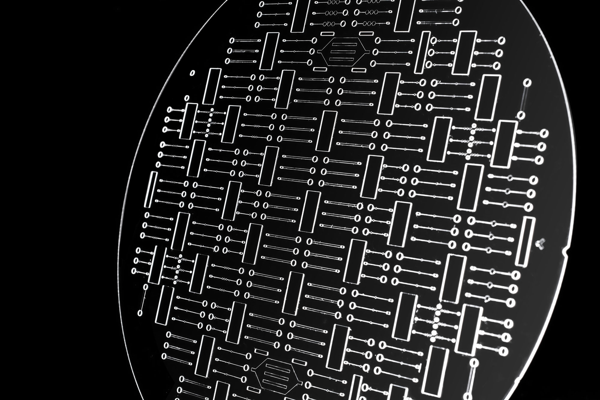
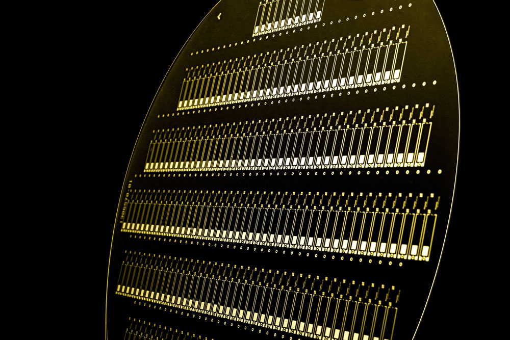
IMT offers leading edge technology solutions by automated and standardized processes by applying MEMS production schemes and equipment on glass wafers.
Thanks to advances in laser machining, photolithography, etching automation, wafer bonding, functionalization, room temperature UV-adhesive bonding and other process improvements, glass and glass-hybrid materials are often both the best-performing and most cost-effective consumable material for Life Science and Diagnostics devices.
IMT has implemented an automated manufacturing line that allows cost effective mass manufacturing of consumables in a variety of glass substrate materials. The Ø200mm wafer automatic production line facilitates deposition and structuring of metallic and dielectric coatings, Wet- and Dry-Etch processes, wafer level fusion or UV-adhesive bonding, integration of electrodes, waveguides, optical filters and surface functionalization.