CIME-P offers Europractice customers access to STMicroelectronics technologies.
For updated technology details, please contact cime-prototypage@grenoble-inp.fr
CIME-P offers Europractice customers access to STMicroelectronics technologies.
For updated technology details, please contact cime-prototypage@grenoble-inp.fr
Several process steps and masking levels are removed from the 28nm bulk process. This compensates the extra cost of the SOI substrate wafers. FD-SOI has lower channel leakage current. Carriers are efficiently confined from source to drain: the buried oxide prevent these carriers to spread into bulk. The process comes with NMOS and PMOS devices including body-bias-voltage scaling from 0V to +2V that helps decreases minimum circuit operating voltage. Standard-cells libraries are characterized over a range of voltages from 300mV to 1.2V.
Transistors can be ideally controlled through independent bias voltages. These body bias techniques allow dynamically modulating the transistor threshold voltage. Dynamic voltage and frequency scaling (DVFS) techniques can be applied more efficiently than alternative processes, therefore achieving high performance at conventional voltages.
28nm CMOS FD-SOI ULP, MS/mmW/RF | |
|---|---|
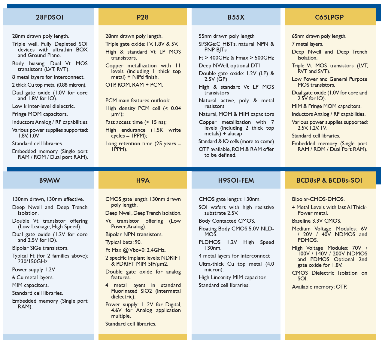
Technology characteristics | CMOS gate length: 28nm drawn poly length Triple well Fully Depleted SOI devices, with ultrathin BOX and Ground Plane Body biasing Dual Vt MOS transistors (LVT, RVT) Dual gate oxide (1.0V for core and 1.8V for IO) Temperature range: -40°C to 125°C Dual-damascene copper for interconnect, low-k dielectric 8 metal layers (8ML) for interconnect, 2 thick Cu top metal (0.880 micron) Low k inter-level dielectric Fringe MoM capacitors Inductors Analog / RF capabilities Various power supplies supported: 1.8V, 1.0V Standard cell libraries (more than 3Mgates/mm2) Embedded memory (Single port RAM / ROM / Dual Port RAM). |
Application area | Internet of Things, Wearable • Ultra-low-voltage operation • FBB optimizes power/performance • Efficient RF and analog integration Automotive • Well-managed leakage in high-temperature environments • High reliability thanks to highly-efficient memories Networking Infrastructure • Energy-efficient multicore • Adapt performance & power to workload via FBB • Excellent performance in memories Consumer Multimedia • Optimized SoC integration (Mixed-signal & RF) • Energy-efficient SoC under all thermal conditions • Optimized leakage in idle mode |
Design Kit version | 1.5.a (Sept. 21) |
Frontend Backend tools | Cadence IC 6.1.7
|
Simulation tools | Analog simulations: Spectre (Cadence), Eldo (Siemens EDA – Siemens EDA), ADS for Momentum & GoldenGate (Keysight)
Digital simulation: Xcelium (Cadence) |
Verification tools | Calibre (Siemens EDA) PVS (Cadence) |
Parasitic extraction tools | StarRCXT (Synopsys), QRC (Cadence) |
Place route tools | Innovus (Cadence), ICC (Synopsys) |
Libraries | CORE cells Libraries: – CORE: General purpose core cells – CLOCK: Buffer cells for clock tree synthesis – PR: Place and route filler cells IO cells Libraries: – 1.8V Digital IOs: – 1.0V, 1.8V, 3.3V Analog IOs: – Body Bias supply pads – Bonding pads and Flip-Chip pads On request: – SHIFT: Level Shifters libraries – CORI: Isolation cells – CORR: Retention cells – Compensation cells – DLL, PLL. |
Turnaround time | Typical leadtime: 24-32 weeks from MPW run deadline to packaged parts |
The BiCMOS055 technology of STMicroelectronics is well adapted for applications that require RF performance for analog part and high performance in digital part..
Bipolar SiGe transistors offer gain and high speed performances for analog devices:
CMOS 55nm transistors enable high speed and high density for digital devices:
55nm BiCMOS SiGe MS/mmW/RF | |
|---|---|
Technology characteristics | CMOS Gate length: 55nm drawn poly length Deep Nwell and Deep Trench Isolation Triple Vt MOS transistors (LVT, RVT and SVT) Low Power and General Purpose MOS transistors Dual gate oxide (1.0V for core and 2.5V for IO) Dedicated process flavors for high performance and for low power Bipolar SiGe-C NPN transistors: High Speed NPN with Ft=320GHz Medium Voltage NPN with Ft=180GHz, and High Voltage NPN Temperature range: -40°C to 175°C Dual-damascene copper for interconnect, low-k dielectric 8 Cu metal layers for interconnect Ultra-thick Cu top metal (3.0 micron) Low k inter-level dielectric MiM capacitors & Fringe MoM capacitors Thin Film Resistors (RFR) Millimiter-wave inductors Analog / RF capabilities Various power supplies supported: 2.5V, 1.2V, 1V Standard cell libraries (more than 700kgates/mm² for high speed gates, more than 970kgates/mm² for high density gates) Embedded memory (Single port RAM / ROM / Dual Port RAM). |
Application area | Optical, Wireless and high performance analogue applications.
|
Design Kit version | 3.1.a (May-20) |
Frontend Backend tools | Cadence IC 6.1.7
|
Simulation tools | Spectre (Cadence), Eldo (Siemens EDA), Hspice (Synopsys), GoldenGate (Keysight) |
Verification tools | Calibre (Siemens EDA), PVS (Cadence) |
Parasitic extraction tools | StarRCXT (Synopsys), QRC (Cadence) |
Place route tools | Innovus (Cadence), ICC (Synopsys) |
Libraries | CORE cells Libraries: – CORE: General purpose core libraries – CORX: Complementary core libraries (complex gates) – CLOCK: Buffer cells and the same for clock tree synthesis – PR: Place and route filler cells IO cells Libraries: – 1.2V, 1.8V, 2.5V, 3.3V, Digital and Analog – Staggered IO pads – bonding pads and Flip-Chip pads. On request: – CORI: isolation cells – CORL: core libraries for low power applications – Level Shifters – compensation cells – LVDS Pads – DLL, PLL. |
Turnaround time | Typical leadtime: 28-36 weeks from MPW run deadline to packaged parts |
The CMOS65LPGP technology has been introduced as general purpose and low power process to address 1.0V and 1.2V applications with 1.2V, 1.8V, 2.5V and 3.3V capable I/Os. The design kit has a large bench of fully characterized devices. The RF kit includes inductors, varactors and MiM capacitors.
65nm CMOS MS/RF, LP/GP | |
|---|---|
Technology characteristics | CMOS gate length: 65nm drawn poly length Deep Nwell and Deep Trench Isolation Triple Vt MOS transistors (LVT, RVT and SVT) Low Power and General Purpose MOS transistors Dual gate oxide (1.0V for core and 2.5V for IO) Dedicated process flavors for high performance and for low power Temperature range: -40°C to 175°C Dual-damascene copper for interconnect, low-k dielectric 7 Cu metal layers for interconnect Low k inter-level dielectric MiM capacitors & Fringe MoM capacitors Inductors Analog / RF capabilities Various power supplies supported: 2.5V, 1.2V, 1V Standard cell libraries (more than 800kgates/mm2) Embedded memory (Single port RAM / ROM / Dual Port RAM). |
Application area | General purpose, Analogue and RF capabilities.
|
Design Kit version | 5.8 (Jul.-19) |
Frontend Backend tools | Cadence IC 6.1.6
|
Simulation tools | Spectre (Cadence), Eldo (Siemens EDA), Hspice (Synopsys), ADS Momentum (Keysight), GoldenGate (Keysight) |
Verification tools | Calibre (Siemens EDA), PVS (Cadence) |
Parasitic extraction tools | StarRCXT (Synopsys), Calibre xRC (Siemens EDA), QRC(Cadence) |
Place route tools | Innovus (Cadence), ICC (Synopsys) |
Libraries | CORE cells Libraries: - CORE: general purpose core libraries - CORI: isolation cells - CORL: core libraries optimized to reduce overall leakage - CORX: complementary core libraries (complex gates) - CLOCK: buffer cells and the same for clock tree synthesis - PR: place and route filler cells - SHIFT : level shifters IO cells Libraries: - 1.2V, 1.8V, 2.5V, 3.3V, 7V Analog IOs - 1.2V, 1.8V, 2.5V, 3.3V Digital IOs - Supply and ground pads - Compensation cells - Bonding pads and Flip-Chip pads On request: - LVDS Pads - PLL. |
Turnaround time | Typical leadtime: 22-26 weeks from MPW run deadline to packaged parts |
The HCMOS9GP technology is the main process for the 130 nm node. It has been introduced as a general‐purpose process to address 1.2V applications with 1.8V or 2.5V capable I/O’s. The Design Kit provides a large bench of fully characterized devices, with standard Core cells and IO cells.
The design kit is provided with fully characterized devices:
130nm HCMOS9GP | |
|---|---|
Technology characteristics | CMOS gate length: 130nm drawn poly length Deep Nwell and Deep Trench Isolation Power supply 1.2V Double Vt transistor offering (Low Leakage , High Speed) Threshold voltages (for 2 families above): VTN = 450/340mV, VTP = 395/300mV Isat (for 2 families above): TN @ 1.2V: 535/670uA/mic TP @ 1.2V: 240/310uA/mic Dual gate oxide (1.2V for core and 2.5V for IO) Temperature range: -40°C to 175°C 6 Cu metal layers for interconnect Low k inter-level dielectric MIM capacitors Standard cell libraries (more than 180kgates/mm2) Embedded memory (Single port RAM / ROM / Dual Port RAM). |
Application area | General purpose analogue/digital.
|
Design Kit version | 9.2
|
Frontend Backend tools | Cadence IC 5.1.41_USR6
|
Simulation tools | Spectre (Cadence), Eldo (Siemens EDA), Hspice (Synopsys)
|
Turnaround time | Typical leadtime: 16-18 weeks from MPW run deadline to packaged parts |
The BiCMOS9MW technology was defined by using the 130 nm HCMOS9 as base process and adds additional levels, in front‐end and back‐end. It has been introduced to address millimeterwave applications (Frequencies up to 77 GHz), wireless communication (around 60GHz for WLAN) and optical communications systems.
130nm BiCMOS9MW SiGe MS/RF | |
|---|---|
Technology characteristics | CMOS Gate length: 130nm drawn, 130nm effective Deep Nwell and Deep Trench Isolation Double Vt transistor offering (Low Leakage , High Speed) Dual gate oxide (1.2V for core and 2.5V for IO) Threshold voltages (for 2 families above): VTN = 450/340mV, VTP = 395/300mV Isat (for 2 families above): TN @ 1.2V: 535/670uA/mic TP @ 1.2V: 240/310uA/mic Bipolar SiGe transistors: High Speed NPN Medium VoltageNPN Typical beta (for 2 families above): 1000/1000 Typical Ft (for 2 families above): 230/150GHz Power supply 1.2V Temperature range: -40°C to 175°C 6 Cu metal layers Low k inter-level dielectric MIM capacitors Standard cell libraries (more than 180kgates/mm2) Embedded memory (Single port RAM / ROM / dual port RAM). |
Application area | RF applications and millimetre-waver application, WLAN, Optical communications.
|
Design Kit version | 3.4 (Oct.-20) |
Frontend Backend tools | Cadence IC 6.1.7
|
Simulation tools | Analog simulations: Spectre (Cadence), Eldo (Siemens EDA – Siemens EDA), Hspice (Synopsys), ADS for Momentum & GoldenGate (Keysight) Digital simulations: Xcelium (Cadence) |
Verification tools | Calibre (Siemens EDA – Siemens EDA), PVS (Cadence) |
Parasitic extraction tools | StarRCXT (Synopsys), QRC (Cadence) |
Place route tools | Innovus (Cadence), ICC (Synopsys) |
Libraries | CORE cells Libraries: – CORE: General purpose core libraries – CLOCK: Buffer cells for clock tree synthesis – PR: Place and route filler cells IO cells Libraries: – 2.5V, 3.3V IO pads, Digital and Analog – Bonding pads and flip-chip pads. |
Turnaround time | Typical leadtime: 16-18 weeks from MPW run deadline to packaged parts |
This technology is intended to serve at best RF ultra low cost applications. H9‐SOI‐FEM is built on the same solid basis of the previous standard H9SOI technology and shares with it the robustness, the capability to address all FEM (stand for Front End Module) applications (RF Switches, PA, LNA) and the expertise in RF SOI process. In addition, H9‐SOI‐FEM technology includes several improvements such as cost‐driven application, performance improvement and a better manufacturing capacity.
130nm HCMOS9‐SOI FEM | |
|---|---|
Technology characteristics | CMOS gate length: 130nm SOI wafers with high resistive substrate 2.5V Body Contacted CMOS Floating Body CMOS 5.0V NLDMOS PLDMOS 1.2V High Speed 130nm CMOSmeta Temperature range: -40°C to 175°C 4 metal layers for interconnect Ultra-thick Cu top metal (4.0 micron) High Linearity MIM capacitor Standard cell libraries. |
Application area | Radio receiver/transceiver.
|
Design Kit version | 14.1
|
Frontend Backend tools | Cadence IC |
Simulation tools | Spectre (Cadence), Eldo (Siemens EDA) |
Verification tools | Calibre (Siemens EDA – Siemens EDA), PVS (Cadence) |
Parasitic extraction tools | QRC (Cadence) |
Place route tools | Innovus (Cadence)
|
Libraries | Core: Libraries general purpose 2.5V IO cells libraries: 1.8V, 2.5V, Digital and Analog pads, flip-chip pads, ESD kit cells. |
Turnaround time | Typical leadtime: 16-18 weeks from MPW run deadline to packaged parts |
This STMicroelectronics technology on the 130nm node, based on the HCMOS9GP DRM, targets the mixed digital analog design with energy management features.
Note: HCMOSA process from STMicroelectronics is presently mainly used for making the OxRAM post-process from CEA-LETI in order to make embedded Non-Volatile Memory (NVM). The metal stack back-end from the ST process is stopped at the last metal layer to allow the OxRAM / NVM post-process deposition by CEA-LETI. All HCMOSA MPW runs are presently offered with this NVM post-process.
Nevertheless, dedicated engineering runs in pure HCMOS9A are still possible to run.
130nm HCMOS9A LP/HV | |
|---|---|
Technology characteristics | CMOS gate length: 130nm drawnpoly length Deep Nwell and Deep Trench Isolation Vt transistor offering (Low Power, Analog) Threshold voltages (for 2 families above): VTN = 700/697mV, VTP = 590/626mV Isat (for 2 families above): TN: 280/658uA/um – TP: 104/333uA/um Bipolar NPN transistors Typical beta: 90 Ft Max @ Vbc=0: 2,4GHz 2 specific implant levels: NDRIFT & PDRIFT MIM 5fF/µm2 Double gate oxide for analog features Temperature range: -40°C to 125°C 4 metal layers in standard Fluorinated SiO2 Inter Metal dielectrics Power supply: 1. 2V for Digital, 4.6V for Analog application multiple Standard cell libraries. |
Application area | Energy harvesting applications, Automous systems.
|
Design Kit version | 10.9 (May-19) |
Frontend Backend tools | Cadence IC 6.1.7
|
Simulation tools | Spectre (Cadence), Eldo (Siemens EDA), Hspice (Synopsys) |
Verification tools | Calibre (Siemens EDA – Siemens EDA), PVS (Cadence) |
Parasitic extraction tools | StarRCXT (Synopsys), QRC (Cadence) |
Place route tools | Innovus (Cadence) |
Libraries | CORE cells Libraries: – CORE: General purpose core libraries – CORX: Complementary core libraries (complex gates). – PR: Place and route filler cells IO cells Libraries: – 1.2V, 1.8V, 4.6V, 20V IO pads, Digital and Analog – Bonding pads and flip-chip pads. On request: – Level Shifters. |
Turnaround time | Typical leadtime: 16-18 weeks from MPW run deadline to packaged parts |
ST Microelectronics « Smart Power » BCD8sP technology combines high power transistors with low power digital and analog devices on a single chip. This technology is dedicated to power management systems, power supplies, motor drivers, amplifiers etc.
0.16µm BCD8sP HV Bipolar-CMOS-DMOS | |
|---|---|
Technology characteristics | Temperature range: -40°C to +175°C 0.16µm Bipolar-CMOS-DMOS 4 metal layers (2 top metal options : Al or CuRDL) Baseline 1.8V CMOS Power devices: 5V / 10V / 18V / 27V / 42V / 60V Dual gate oxide process: 1.8V CMOS, 5V CMOS & Power Devices Optional DTI for lateral isolation |
Application area | Hard disk drivers, DC-DC converters, Power management.
|
Design Kit version | 2.4 (2016) |
Frontend Backend tools | Cadence IC 6.1.6
|
Simulation tools | Spectre (Cadence), Eldo (Siemens EDA) |
Verification tools | Calibre (Siemens EDA) |
Parasitic extraction tools | StarRCXT (Synopsys) |
Libraries | – Pcells (bipolars, MOSs, diodes, capacitors, resistors) – Standard cells (1.8V, 5V) – Basic IOs (3.3V, 5V) – Power generator – Macrocells ESD – Antifuse (on request) |
Turnaround time | Typical leadtime: 18-24 weeks from MPW run deadline to packaged parts |
ST Microelectronics « Smart Power » BCD8s-SOI technology is dedicated to high voltage applications on SOI substrates. This technology is convenient and even mandatory in case of MEMS & micro-mirror driver, consumer and automotive audio amplifiers, automotive sensor interface, 3D Ultrasound etc.
0.16µm BCD8s-SOI HV Bipolar-CMOS-DMOS | |
|---|---|
Technology characteristics | Temperature range: -40°C to +175°C 0.16µm Bipolar-CMOS-DMOS 4 Metal Levels with last Al Thick Power metal Baseline 3.3V CMOS Medium Voltage Module: 6V / 20V / 40V NMOS and PMOS High Voltage Module: 70V / 100V / 140V / 200V NMOS and PMOS Optional 2nd gate oxide for 1.8V CMOS Dielectric Isolation on SOI Available memory: OTP |
Design Kit version | 2.1 (2017) |
Frontend Backend tools | Cadence IC 6.1.7 |
Simulation tools | Spectre (Cadence), Eldo (Siemens EDA) |
Verification tools | Calibre (Siemens EDA) |
Parasitic extraction tools | StarRCXT (Synopsys) |
Libraries | Power devices (Power generator for specific needs available through CMP) Standard cells (1.8V, 3.3V) Pcells (bipolars, diodes, capacitors, resistors) Macrocell ESD, Antifuse (optional). |
Turnaround time | Typical leadtime: 18-24 weeks from MPW run deadline to packaged parts |
Copper pillars are manufactured at wafer-level by STMicroelectronics. This interconnection is composed of an Under Bump Mettalization (UBM), upon which a pillar of copper is grown, a capping of Sn/Ag allows the die to be assembled on a substrate by reflow process. The dimensions of this copper pillar are approximately 62 µm in diameter for 65 µm in height, thus allowing a fine pitch (down to 90 µm).
Accessibility conditions: