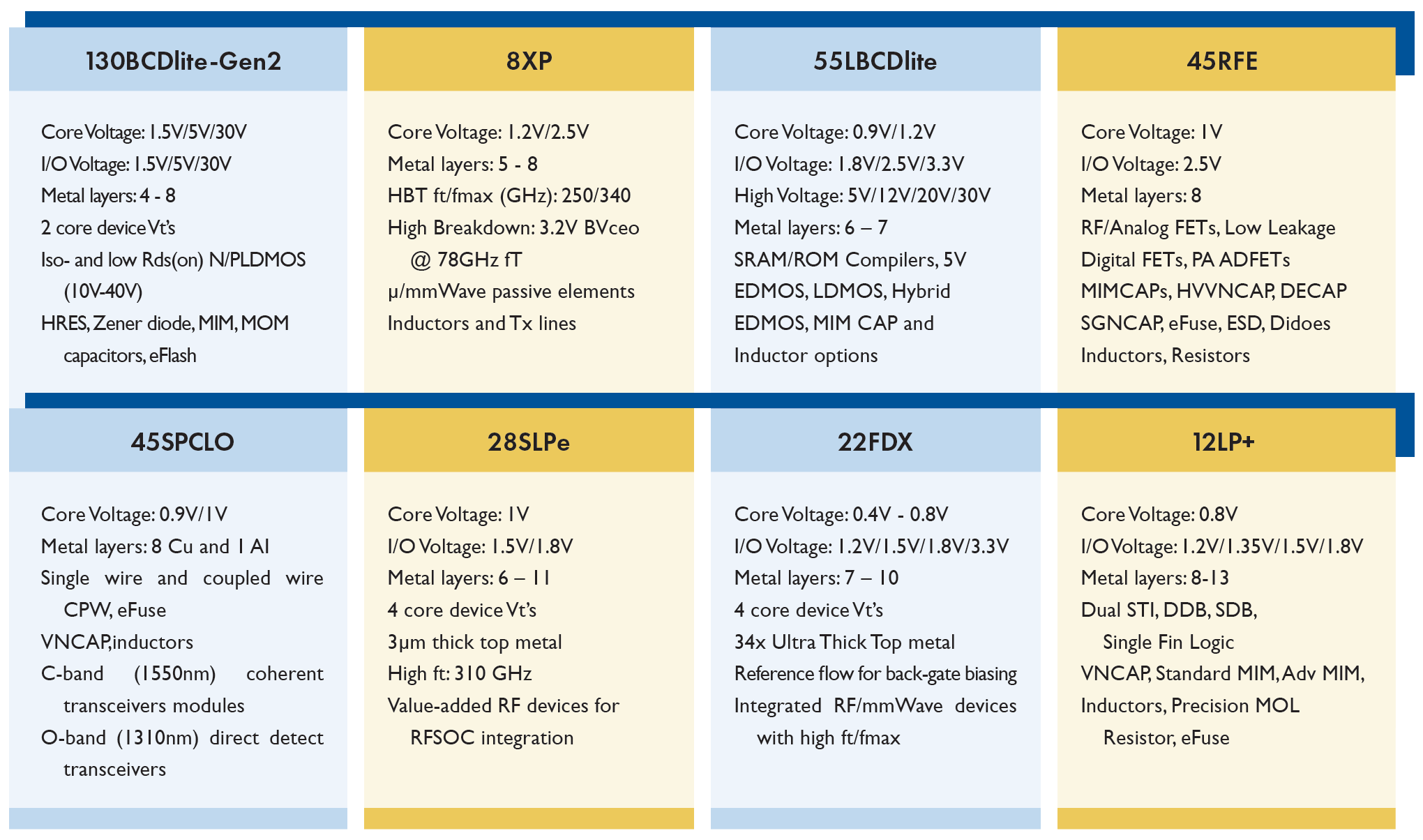
Europractice provides access to the following GlobalFoundries technologies.

Europractice provides access to the following GlobalFoundries technologies.
GF’s SiGe 8XP technology drawn at 130nm features low noise figures, high linearity, gain, breakdown and operating voltages, together with simplified impedance matching and excellent thermal stability. Advanced SiGe heterojunction bipolar transistors (HBTs) provide superior low-current and high-frequency performance while enabling the technology to operate at high junction temperatures.
GF SiGe 8XP | |
|---|---|
Technology characteristics | Core voltage: 1.2V / 2.5V I/O voltage: 1.5 / 1.8V / 2.5V / 3.3V TSV Metal layers: 5 – 7 of Cu and AI Thick Al and Cu “MA” add-on module for high Q inductors Forward Bias, PIN and Schottky Barrier Diodes High performance SiGe NPN transistors (fT/fmax 250/340GHz) High breakdown fT= 78GHz, 3.2V BVceo Temperature Range: -55°C to 125°C Device offerings: SchottkyDiode, P+ poly resistors, Thin oxide NMOS varactor/ decoupling capacitor, Spiral inductors, Transmission lines, mmWave passive elements, eFuse, Triple-well NFETs, PIN Diode, Hyper abrupt (HA) varactor, MIM capacitor, Dual MIM (3 fF/μm2), High-RsRR poly resistor, TaNmetal KQ resistor, True triple well (T3) FET |
Wafer size | 8inch |
Manufacturing location | Fab9 – Burlington, Vermont, USA
|
Deliverables
| 45-50 Dies (depends on 3rd party packaging services) |
Signoff tools
| Cadence, Siemens EDA
|
Foundational IPs
| Standard cell libraries: GLOBALFOUNDRIES GPIO : GLOBALFOUNDRIES SRAM : ARM / GLOBALFOUNDRIES The ARM IPs have to be requested directly at ARM via DesignStart portal For GLOBALFOUNDRIES IPs contact Fraunhofer IIS |
Dummy filling
| To be done by the customer
|
MPW block size
| 12mm² |
Turnaround time
| ca. 6 months
|
mini@sic characteristics
| Supported only for Universities and Research Institutes Block size: min. 2mm² |
Bumping
| Cu Pillar and SnAg
|
The GF 130BCDLite process is tailored for cost-effective mobile/consumer applications: DC-DC, AC-DC, PMIC, Wireless and Quick Charging.
GF 130BCDLite – Gen2 | |
|---|---|
Technology characteristics | Core and I/O Voltage: 1.5V/5V/12-40V 8-12 Ω-cm p-type substrate (noise isolation) Poly layers: 1, Metal layers: 4-8 of Cu Top metal thickness: 30kA and/or 9kA Recommended metal stack on MPW: 1P7M TM30K Metal: Cu, AI(RDL) Device offeringss: High gain MOSFETs with Regular and NativeVt, BJTs, Diodes, Single Mask MIM, Resistors, eFuse, Inductors, ESD, Pads. RF Devices: MOSFETs, LDMOS, Capacitors and Diodes Special devices: MTP, OTP, eFlash Passivation: Single or Dual |
Wafer size | 12inch |
Manufacturing location | Fab7 – Woodlands, Singapore
|
Deliverables
| 45-50 Dies (depends on 3rd party packaging services)
|
Signoff tools
| Cadence, Synopsys, Siemens EDA
|
Foundational IPs
| Standard cell libraries: ARM GPIO : GLOBALFOUNDRIES SRAM : ARM The foundational IPs have to be requested directly at the IP vendor: – ARM via DesignStart portal – For GLOBALFOUNDRIES GPIO contact Fraunhofer IIS |
Dummy filling
| To be done by the customer
|
MPW block size
| 25mm²
|
Turnaround time
| ca. 5 months
|
mini@sic characteristics
| Supported only for Universities and Research Institutes Block size: min. 4mm² |
Bumping
| Solder bump
|
Industry’s first 55BCDLite technology (300mm, Cu BEOL). 55BCDlite is built on top of 55LPx platform. It delivers optimal performance for mobile audio amplifiers and smart phone power solutions enabled by its industry leading lowest RdsOn versus BVdss breakdown voltage.
GF 55BCDLite | |
|---|---|
Technology characteristics | Core Voltage: 0.9V/1.2V I/O Voltage: 1.8V/2.5V/3.3V High Voltage: 5V/10/12V/20V/30V -40C to 125C 4 – 9 copper metals Minimum drawn gate length = 0.06μm Twin or triple well CMOS technology on p-substrate Core FETs: SLVTs, LVTs, SHVTs, HVTs and StdVTs 5V CMOS (gate oxide 25nm n/p) 5V Isolated Low Rdson EDMOS 8/10/12V Isolated Low Rdson EDMOS, 12V Regular EDMOS Switching 20V EDMOS, Low TCR TaN Resistor, AVT FETs, FHRES Legacy MIMCAP and inductor option, High Resistor options |
Wafer size | 12inch |
Manufacturing location | Fab7 – Woodlands, Singapore |
Deliverables
| 45-50 Dies (depends on 3rd party packaging services)
|
Signoff tools
| Cadence, Siemens EDA |
Foundational IPs
| Standard cell libraries: GF GPIO: GF eFuse: GF |
Dummy filling
| To be done by the customer
|
MPW block size
| 12mm² |
Turnaround time
| ca. 6 months
|
mini@sic characteristics
| Supported only for Universities and Research Institutes Block size: min. 2mm² |
Bumping
| Cu Pillar and SnAg
|
45RFE is a 45 nm generation, SOI, CMOS technology that supports application-specific integrated circuit (ASIC) designs, SRAM, and custom logic designs.
Ground up mmWave technology based on 45RFSOI and incorporates key RF devices (RVT, ADNFET) with high ft and fmax. SOI transistors can be stacked, enables higher voltage and power handling. It provides additional RF benefits with reduced parasitics , higher Q and lower loss with Increased isolation and linearity with Higher efficiency antenna on chip.
GF 45RFE | |
|---|---|
Technology characteristics | Core Voltage: 1V I/O Voltage: 2.5V Hgate FETs, Low leakage digital FETs, ADNFET Thick & Thin gate oxide FETs, Resistors, Inductors, and Diodes Capacitors, Substrate HR + processing ~1.5K Ohm cm, ESDs Two BEOL STACK options 8 Levels of Cu Wiring (including 2x 3um Cu wires and 2um Al) Operating junction temperature range of -40°C to 125°C VDD of 1.0 V (thin oxide), Shallow trench isolation (STI) Electrically programmable fuse (eFUSE) RF Features: High and low density MIM capacitors High-value resistor 1.5K Ohms/square, BEOL stacks – 8 level ADFETs for RF power amplification |
Wafer size | 12inch |
Manufacturing location | Fab8 – USA |
Deliverables
| 45-50 Dies (depends on 3rd party packaging services)
|
Signoff tools
| Cadence, Siemens EDA |
Foundational IPs
| Standard cell libraries: GF GPIO: GF eFuse: GF |
Dummy filling
| To be done by the customer
|
MPW block size
| 12mm² |
Turnaround time
| ca. 6 months
|
mini@sic characteristics
| Supported only for Universities and Research Institutes Block size: min. 1mm² |
Bumping
| Cu Pillar and SnAg
|
45RFSOI takes advantage of a 45nm partially-depleted SOI server-class technology base that has been extensively evaluated for use in mmWave applications and in high volume production at multiple GF fabs since 2008. Today, this baseline process has RFcentric enablement, topped with device and technology additions, including thick copper and dielectric back-end-of-line (BEOL) features which enable 45RFSOI to handle the demanding performance requirements of 5G solutions.
GF 45RFSOI | |
|---|---|
Technology characteristics | High-resistivity substrate ≥7500 Ω-cm Three BEOL STACK options: 7 or 8 Levels of Cu Wiring and Thick Al LD or LB Operating junction temperature: -40°C to 125°C VDD of 0.9 V or 1.0 V (thin oxide) Two gate oxide thicknesses High density / High Q MIMcap, High-value resistor RF and mmWave offering: Inductors, Microstrip, Coplanar Waveguides, Passives Fuse: eFuse |
Wafer size | 12inch |
Manufacturing location | FAB8 – USA |
Deliverables
| 45-50 Dies (depends on 3rd party packaging services)
|
Signoff tools
| Cadence, Siemens EDA
|
Foundational IPs
| Standard cell libraries: ARM GPIO : ARM SRAM : N/A The foundational IPs have to be requested directly at ARM via DesignStart portal |
Dummy filling
| To be done by the customer
|
MPW block size
| 12mm² |
Turnaround time
| ca. 5.5 months
|
mini@sic characteristics
| Supported for universities and research institutes Block size: min. 1mm2 |
Bumping
| Available only for general MPW (Cu Pillar and SnAg)
|
45SPCLO is a 45 nm generation, SOI, CMOS technology that supports (ASIC) designs and custom logic designs. It offers power, area, and performance advantages and efficiency providing more data per watt per fibre per Laser. Monolithic integration of RF, digital and Si-Photonic circuits with higher energy efficiency and higher modulation speed. Ideal for applications like Automotive Lidar, IoT, Cloud, Frictionless Networking, Virtualization and Hierarchical AI.
GF 45 SPCLO Silicon-Photonics | |
|---|---|
Technology characteristics | CMOS technology substrate resistivity is in the range of 9-18 ohm-cm Core Voltages: 0.9V, 1V, IO Voltages: 1.5V, 1.8V 1.12 nm thin gate oxide for 0.9 V 2.5 nm thick gate oxide for 1.5 V and 1.8 V Mini. lithographic image of 40 nm (gate only) Operating junction temperature: -40°C to 125°C One BEOL STACK options: 9LM Metallization stack Seven levels of all-copper global metal 1x, 2x, and 8x thick wires at relaxed pitches Low-K and TEOS/FTEOS Inter Level Dielectrics Planarized passivation and interlevel dielectrics High-value resistor 1.5K Ohms/square |
Photonic offering
| C-band (1550 nm) coherent transceivers modules O-band (1310 nm) direct detect transceivers |
Photonic waveguide
| Polarization splitter & rotator, modulators, detectors Phase shifter, connection options (Polymer bundle or Fiber Butt) Vertical grating incoupler: iograt |
Device offering
| Regular Vt, floating-body FETs Ultrahigh Vt, floating-body FETs Analog, body-contacted FETs Thick-oxide, body-contacted FETs Precision resistors,Thick-oxide decoupling capacitor Efuse, Ge EPI Photo diode, Nitride wave guide in MOL |
Wafer size
| 12inch
|
Manufacturing location
| Fab8 – Malta, New York, USA
|
Deliverables
| 45-50 Dies (depends on 3rd party packaging services)
|
Signoff tools
| Cadence, Synopsys, Siemens EDA
|
Dummy filling
| By customer
|
MPW block size
| 25mm² with fix dimensions of 5mm x 5mm
|
MPW Turnaround time
| 5-6 months
|
Mini@sic characteristics
| Supported Block size: 5mm x 2.455mm or 2.455mm x 5mm (Pre-Shrink die size) |
Bumping
| Upon request |
The GLOBALFOUNDRIES 28SLPe process technology platform is optimized for power, performance and die cost. 28SLPe utilizes optical 0.9x shrink of designs drawn at 32nm dimensions.
GF 28SLPe | |
|---|---|
Technology characteristics | Core voltage:1V I/O voltage:1.5V/1.8V 1 poly and 6 – 11 levels of all Copper metal, plus Aluminum top layer metal 3 μm thickness copper layer for Inductors Temperature Range: -40°C to 125°C Vt Options: SLVt, LVt, RVt, HVt Device offerings: Standard FETs, Zero-Vt NFETs, BJTs, eFuse Resisitors:N+,P+ diffusion and N+,P+ polysilicon silicided,Nwell N+ diffusion and p+ polysilicon OP,High-precision p+ polysilicon OP Capacitors:Thin, Medium (EG) oxide NCAP, PCAP, VNCAP or APMOM Different devices available for eFlash designs |
Recommended Metal Stack on MPW
| Option #2 (6U1x_2T8x_LB)
|
Wafer size | 12inch |
Manufacturing location | Fab1 – Dresden, Germany
|
Deliverables
| 45-50 Dies (depends on 3rd party packaging services) |
Signoff tools
| Cadence, Synopsys, Siemens EDA
|
Foundational IPs
| Standard cell libraries: ARM GPIO : Aragio SRAM : ARM The foundational IPs have to be requested directly at the IP vendor: – ARM via DesignStart portal – For Aragio GPIO contact Jennifer Blakeman |
Dummy filling
| To be done by the customer
|
MPW block size
| 9mm² with a min. edge length of 1mm, flexible aspect ratio
|
Turnaround time
| ca. 4.5 months
|
mini@sic characteristics
| Supported only for Universities and Research Institutes Block size: min. 1mm² with a min. edge length of 1mm, flexible aspect ratio |
Bumping
| Cu Pillar and SnAg
|
GLOBALFOUNDRIES 22nm FD-SOI transistor technology delivers FinFET-like performance and energy-efficiency, including up to 70% lower power vs. 28nm. The simultaneous high Ft /high Fmax, high self gain and high current efficiency of 22FDX enables efficient, ultra low power analog/RF/mmWave designs. The process offers reference flow for back-gate biasing and RF BEOL with ultra thick metal stacks. The eMRAM module supports fully integrated, versatile memory for storage and compute for IoT and MCU.
GF 22FDX | |
|---|---|
Technology characteristics | Non-shrink process Core voltage: 0.8V I/O voltage: 1.2V/1.5V/1.8V, LDMOS @ 3.3V/5V/6.5V 1 poly and 6 – 10 levels of all copper metal, plus thick aluminum top layer metal 6 Vt options: eLVt, SLVt, LVt, RVt, HVt, UHVt Qualified for Automotive Grade 1 (-40°C to 150°C) Device offerings: Standard FETs, Diodes, BJTs, Passives (Resistors, AP/SP MOM, eFuse, Varactor, Parasitic Caps), SRAM (ULL, HD, SP, DP), ESD RF/mmWave support: FETs, Resistor, Inductor, Varactor, APMOM, Tx Line Special offering: eMRAM |
Wafer size | 12inch |
Manufacturing location | Fab1 – Dresden, Germany
|
Deliverables
| 45-50 Dies (depends on 3rd party packaging services) |
Signoff tools
| Cadence, Synopsys, Siemens EDA
|
Foundational IPs
| Standard cell libraries: Synopsys GPIO : Synopsys SRAM : Synopsys The foundational IPs have to be requested directly at Synopsys via DesignWare IP portal |
Double patterning and Dummy filling
| To be done by the customer
|
MPW block size
| 9mm² with a min. edge length of 1mm, flexible aspect ratio
|
Turnaround time
| ca. 3.5 months
|
mini@sic characteristics
| Supported only for Universities and Research Institutes Block size: min. 1mm² with a min. edge length of 1mm, flexible aspect ratio |
Bumping
| Cu Pillar and SnAg
|
The 12nm GLOBALFOUNDRIES 12LP+ FinFET process technology platform is ideal for high-performance, power-efficient SoCs in demanding, high-volume applications. 3D FinFET transistor technology provides best-in-class performance and power with significant cost advantages from 12nm area scaling. The 12LP+ technology can provide up to 20% higher device performance and 36% lower total power compared to the 12LP technology.
GF 12LP+ | |
|---|---|
Technology characteristics | Based on 14LPP technology Dual STI Core voltage: 0.8V I/O voltage: 1.2V / 1.35V / 1.5V / 1.8V BEOL Stack options: 8ML / 9ML / 10ML / 11ML / 13ML SLVT, LVT, RVT, HVT, DDB, SDB, Single Fin Logic Device offerings: ESD diodes, vertical BJT, VNCAP, Standard MIM, Adv MIM, Inductors, Precision MOL Resistor, eFuse |
Wafer size | 12inch |
Manufacturing location | Fab8 – Malta, New York, USA
|
Deliverables
| 45-50 Dies (depends on 3rd party packaging services) |
Signoff tools
| Cadence, Synopsys, Siemens EDA
|
Foundational IPs
| Standard cell libraries: ARM GPIO : ARM SRAM : ARM The foundational IPs have to be requested directly at the IP vendor ARM via DesignStart portal |
Double patterning and Dummy filling
| To be done by the customer
|
MPW block size
| 9mm² with a min. edge length of 1mm, flexible aspect ratio
|
Turnaround time
| ca. 5.5 months
|
mini@sic characteristics
| Supported only for Universities and Research Institutes Block size: min. 1mm² with a min. edge length of 1mm, flexible aspect ratio |
Bumping
| Cu Pillar and SnAg
|