
ams OSRAM manufactures high performance analog semiconductors that solve its customers’ most challenging problems with innovative solutions.
Here are some highlights from the ams OSRAM technology portfolio.
Europractice partners CIME-P and Fraunhofer provide access to the following ams technologies:
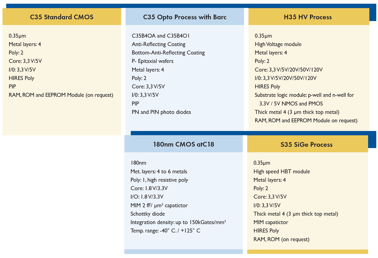
180nm CMOS atC18c | |
|---|---|
Technology characteristics | Met. layer(s): 4 to 6 metals Poly layer(s): 1, high resistive poly Available I/O: I/O cell library with digital pads is available 1.8V, 3.3V Temp. range: -40° C. / +125° C Supply voltage: 1.8 V to 3.3V |
Special features | High performance Mixed analog/digital process |
Application area | Mixed signal analog/digital, large digital designs, system on chip |
Design Kit version | 4.16 ISR 10 |
Frontend Backend tools | Cadence IC 6.1.8 → analog and digital Synopsys → digital |
Simulation tools | Spectre, Xcelium (Cadence) Safe Operating Area Checks (SOAC) → Spectre Asserts |
Verification tools | LVS → Assura (Cadence), Calibre (Siemens Mentor) DRC → Calibre (Siemens Mentor) |
Parasitics extraction tools
| QRC (Cadence) |
Place route tools | Innovus (Cadence) |
IR / EM analysis | Voltus (Cadence) |
Turnaround time | Typical leadtime: 10-12 weeks from MPW run deadline to packaged parts |
0.35µm CMOS C35B4C3 | |
|---|---|
Technology characteristics | Met. layer(s): 4 Poly layer(s): 2, high resistive poly Maximum die size: 2cm x 2cm DLP Usable cells: about 300 digital cells Available I/O: I/O cell library with digital pads is available 3.3V, 3V/5V, 5V with internal level shifters Temp. range: -40° C. / +125° C Supply voltage: 5V or 3.3V |
Special features | High performance analog/digital process
|
Application area | Mixed signal analog digital, large digital designs, system on chip
|
Design Kit version | 4.10 ISR 15
|
Frontend Backend tools | Cadence IC 6.1.6 |
Simulation tools | Spectre (Cadence), Eldo (Siemens EDA), Hspice (Synopsys)
|
Verification tools | Assura (Cadence), Calibre (Siemens EDA)
|
Parasitic extraction tools
| QRC (Cadence) |
Place route tools | Encounter Digital Implementation (Cadence) |
Libraries | Analog libraries: – A_CELLS: Low Voltage Analog Standard Cells – ESDLIB, PRIMLIB, PRIMLIBRF: Primitive Devices – IOLIB_ANA: Analog I/O pads & Power Supply Pads – IOLIBC_ANA: Core Limited Analog I/O pads & Power Supply Pads – IOLIB_ANA_3B: 3-Bus Analog I/O pads & Power Supply Pads – SPIRALS_4M, SPIRALSD_4M : Inductors Digital libraries: – CORELIB: 3.3V Digital Standard Cells – CORELIB_V5: 5V Digital Standard Cells – CORELIB_3B: Digital Standard Cells with 3 Busses (VDD, VSS, GND) – CORELIBD: Dense 3.3V Digital Standard Cells – IOLIB_4M: Digital Input/Output/Bidirectional buffers & Power Pads – IOLIBC: Core Limited Digital Input/Output/Bidirectional buffers & Power Pads – IOLIB_V5: Digital Input/Output/Bidirectional buffers & Power Pads; 5V Supply – IOLIB_3B: 3-Bus Digital Input/Output/Bidirectional buffers & Power Pads |
Turnaround time | Typical leadtime: 10-12 weeks from MPW run deadline to packaged parts
|
0.35µm CMOS C35B4E3 | |
|---|---|
Technology characteristics | Embedded Flash Met. layer(s): 4 Poly layer(s): 2 Maximum die size: 2cm x 2cm Usable cells: about 300 digital cells Available I/O: I/O cell library with digital pads is available 3V, 3V/5V, 5V with internal level shifters Temp. range: -40° C. / +125° C Supply voltage: 5V or 3.3V |
Special features | High performance analog/digital process embedding Flash/EEPROM |
Application area | The process is fully compatible with C35B4C3 Mixed signal analog digital, large digital designs, system on chip |
Design Kit version | 4.10 ISR 15 |
Frontend Backend tools | Cadence IC 6.1.6 |
Simulation tools | Spectre (Cadence), Eldo (Siemens EDA), Hspice (Synopsys)
|
Verification tools | Assura (Cadence), Calibre (Siemens EDA)
|
Parasitics extraction tools
| QRC (Cadence) |
Place route tools | Encounter Digital Implementation (Cadence) |
Libraries | Analog libraries: – A_CELLS: Low Voltage Analog Standard Cells – ESDLIB, PRIMLIB, PRIMLIBRF: Primitive Devices – IOLIB_ANA: Analog I/O pads & Power Supply Pads – IOLIBC_ANA: Core Limited Analog I/O pads & Power Supply Pads – IOLIB_ANA_3B: 3-Bus Analog I/O pads & Power Supply Pads – SPIRALS_4M, SPIRALSD_4M: Inductors Digital libraries: – CORELIB: 3.3V Digital Standard Cells – CORELIB_V5: 5V Digital Standard Cells – CORELIB_3B: Digital Standard Cells with 3 Busses (VDD, VSS, GND) – CORELIBD: Dense 3.3V Digital Standard Cells – IOLIB_4M: Digital Input/Output/Bidirectional buffers & Power Pads – IOLIBC: Core Limited Digital Input/Output/Bidirectional buffers & Power Pads – IOLIB_V5: Digital Input/Output/Bidirectional buffers & Power Pads; 5V Supply – IOLIB_3B: 3-Bus Digital Input/Output/Bidirectional buffers & Power Pads |
Turnaround time | Typical leadtime: 10-12 weeks from MPW run deadline to packaged parts
|
0.35µm CMOS RF C35B4M3 | |
|---|---|
Technology characteristics | Same as C35B4C3 with Thick Metal module instead of Metal 4 module and with MIM capacitor module Poly layer(s): 2, high resistive poly Maximum die size: 2cm x 2cm Usable cells: about 300 digital cells Available I/O: I/O cell library with digital pads is available 3V, 3V/5V, 5V with internal level shifters Temp. range: -40° C. / +125° C Supply voltage: 5V or 3.3V |
Special features | High performance analog/digital/RF process |
Application area | Mixed signal analog digital, large digital designs, system on chip, RF |
Design Kit version | 4.10 ISR 15 |
Frontend Backend tools | Cadence IC 6.1.6 |
Simulation tools | Spectre (Cadence), Eldo (Siemens EDA), Hspice (Synopsys)
|
Verification tools | Assura (Cadence), Calibre (Siemens EDA)
|
Parasitics extraction tools
| QRC (Cadence) |
Place route tools | Encounter Digital Implementation (Cadence) |
Libraries | Analog libraries: – A_CELLS: Low Voltage Analog Standard Cells – ESDLIB, PRIMLIB, PRIMLIBRF: Primitive Devices – IOLIB_ANA: Analog I/O pads & Power Supply Pads – IOLIBC_ANA: Core Limited Analog I/O pads & Power Supply Pads – IOLIB_ANA_3B: 3-Bus Analog I/O pads & Power Supply Pads – SPIRALS_4M, SPIRALSD_4M, SPIRALS_4M_THICKMET4: Inductors Digital libraries: – CORELIB: 3.3V Digital Standard Cells – CORELIB_V5: 5V Digital Standard Cells – CORELIB_3B: Digital Standard Cells with 3 Busses (VDD, VSS, GND) – CORELIBD: Dense 3.3V Digital Standard Cells – IOLIB_4M: Digital Input/Output/Bidirectional buffers & Power Pads – IOLIBC: Core Limited Digital Input/Output/Bidirectional buffers & Power Pads – IOLIB_V5: Digital Input/Output/Bidirectional buffers & Power Pads; 5V Supply – IOLIB_3B: 3-Bus Digital Input/Output/Bidirectional buffers & Power Pads |
Turnaround time | Typical leadtime: 10-12 weeks from MPW run deadline to packaged parts
|
0.35µm CMOS Opto C35B4O1 | |
|---|---|
Technology characteristics | This 0.35 CMOS-Opto process is offered in each 0.35 CMOS run (C35B4C3). This is a ARC (Anti Reflective Coating) option. Anti-Reflective Coating (ARC) allows a higher photo-sensitivity than C35B4C3. P-Epi wafers for lowering current leakage in the diode (lower dark current). The C35B4O1 is with 4 layers metal available for prototyping and low volume production. Met. layer(s): 4 Poly layer(s): 2 Maximum die size: 2cm x 2cm DLP Usable cells: about 300 digital cells Available I/O: I/O cell library with digital pads is available 3V, 3V/5V, 5V with internal level shifters Temp. range: -40° C. / +125° C Supply voltage: 5V or 3.3V |
Special features | High performance analog/digital process + anti-reflective coating for optical devices |
Application area | Provides enhanced optical sensitivity for embedded photodiodes and high density CMOS camera products. |
Design Kit version | 4.10 ISR 15 |
Frontend Backend tools | Cadence IC 6.1.6 |
Simulation tools | Spectre (Cadence), Eldo (Siemens EDA), Hspice (Synopsys)
|
Verification tools | Assura (Cadence), Calibre (Siemens EDA)
|
Parasitics extraction tools
| QRC (Cadence) |
Place route tools | Encounter Digital Implementation (Cadence) |
Libraries | Analog libraries: – A_CELLS: Low Voltage Analog Standard Cells – ESDLIB, PRIMLIB, PRIMLIBRF: Primitive Devices – IOLIB_ANA: Analog I/O pads & Power Supply Pads – IOLIBC_ANA: Core Limited Analog I/O pads & Power Supply Pads – IOLIB_ANA_3B: 3-Bus Analog I/O pads & Power Supply Pads – SPIRALS_4M, SPIRALSD_4M : Inductors Digital libraries: – CORELIB: 3.3V Digital Standard Cells – CORELIB_V5: 5V Digital Standard Cells – CORELIB_3B: Digital Standard Cells with 3 Busses (VDD, VSS, GND) – CORELIBD: Dense 3.3V Digital Standard Cells – IOLIB_4M: Digital Input/Output/Bidirectional buffers & Power Pads – IOLIBC: Core Limited Digital Input/Output/Bidirectional buffers & Power Pads – IOLIB_V5: Digital Input/Output/Bidirectional buffers & Power Pads; 5V Supply – IOLIB_3B: 3-Bus Digital Input/Output/Bidirectional buffers & Power Pads |
Turnaround time | Typical leadtime: 10-12 weeks from MPW run deadline to packaged parts
|
0.35µm CMOS Opto BARC C35B4OA | |
|---|---|
Technology characteristics | This 0.35 CMOS-Opto option is offered in each 0.35 CMOS run (C35B4C3), this is a BARC (Bottom Anti Reflective Coating) option. Botton Anti-Reflective Coating (BARC) allows a higher sensitivity than ARC. P-Epi wafers for lowering current leakage in the diode (lower dark current). The C35B4OA is with 4 metal layers available for prototyping and low volume production. Met. layer(s): 4 Poly layer(s): 2 Maximum die size: 2cm x 2cm DLP Usable cells: about 300 digital cells Available I/O: I/O cell library with digital pads is available 3V, 3V/5V, 5V with internal level shifters Temp. range: -40° C. / +125° C Supply voltage: 5V or 3.3V |
Special features | High performance analog/digital process + bottom anti-reflective coating for optical devices. |
Application area | Provides enhanced optical sensitivity for embedded photodiodes and high density CMOS camera products. |
Design Kit version | 4.10 ISR 15 |
Frontend Backend tools | Cadence IC 6.1.6 |
Simulation tools | Spectre (Cadence), Eldo (Siemens EDA), Hspice (Synopsys)
|
Verification tools | Assura (Cadence), Calibre (Siemens EDA)
|
Parasitics extraction tools
| QRC (Cadence) |
Place route tools | Encounter Digital Implementation (Cadence) |
Libraries | Analog libraries: – A_CELLS: Low Voltage Analog Standard Cells – ESDLIB, PRIMLIB, PRIMLIBRF: Primitive Devices – IOLIB_ANA: Analog I/O pads & Power Supply Pads – IOLIBC_ANA: Core Limited Analog I/O pads & Power Supply Pads – IOLIB_ANA_3B: 3-Bus Analog I/O pads & Power Supply Pads – SPIRALS_4M, SPIRALSD_4M: Inductors Digital libraries: – CORELIB: 3.3V Digital Standard Cells – CORELIB_V5: 5V Digital Standard Cells – CORELIB_3B: Digital Standard Cells with 3 Busses (VDD, VSS, GND) – CORELIBD: Dense 3.3V Digital Standard Cells – IOLIB_4M: Digital Input/Output/Bidirectional buffers & Power Pads – IOLIBC: Core Limited Digital Input/Output/Bidirectional buffers & Power Pads – IOLIB_V5: Digital Input/Output/Bidirectional buffers & Power Pads; 5V Supply – IOLIB_3B: 3-Bus Digital Input/Output/Bidirectional buffers & Power Pads |
Turnaround time | Typical leadtime: 10-12 weeks from MPW run deadline to packaged parts
|
0.35µm BiCMOS SiGe S35D4M5 | |
|---|---|
Technology characteristics | Met. layer(s): 4, thick metal MIM capacitor Poly layer(s): 2, high resistive poly Maximum die size: 2cm x 2cm Usable cells: about 300 digital cells Available I/O: I/O cell library with digital pads is available 3V, 3V/5V, 5V with internal level shifters Temp. range: -40° C. / +125° C Supply voltage: 5V or 3.3V |
Special features | High performance analog/RF/digital process |
Application area | Mixed signal analog/RF/digital, large digital designs, system on chip |
Design Kit version | 4.10 ISR 15 |
Frontend Backend tools | Cadence IC 6.1.6 |
Simulation tools | Spectre (Cadence), Eldo (Siemens EDA), Hspice (Synopsys)
|
Verification tools | Assura (Cadence), Calibre (Siemens EDA)
|
Parasitics extraction tools
| QRC (Cadence) |
Place route tools | Encounter Digital Implementation (Cadence) |
Libraries | Analog libraries: – A_CELLS: Low Voltage Analog Standard Cells – ESDLIB, PRIMLIB, PRIMLIBRF: Primitive Devices – IOLIB_ANA: Analog I/O pads & Power Supply Pads – IOLIBC_ANA: Core Limited Analog I/O pads & Power Supply Pads – IOLIB_ANA_3B: 3-Bus Analog I/O pads & Power Supply Pads – RFPADS_4M, RFPADS_3B_4M: RF Pads – SPIRALS_4M, SPIRALSD_4M: Inductors Digital libraries: – CORELIB: 3.3V Digital Standard Cells – CORELIB_V5: 5V Digital Standard Cells – CORELIB_3B: Digital Standard Cells with 3 Busses (VDD, VSS, GND) – CORELIBD: Dense 3.3V Digital Standard Cells – IOLIB_4M: Digital Input/Output/Bidirectional buffers & Power Pads – IOLIBC: Core Limited Digital Input/Output/Bidirectional buffers & Power Pads – IOLIB_V5: Digital Input/Output/Bidirectional buffers & Power Pads; 5V Supply – IOLIB_3B: 3-Bus Digital Input/Output/Bidirectional buffers & Power Pads |
Turnaround time | Typical leadtime: 16-18 weeks from MPW run deadline to packaged parts |
0.35µm CMOS High Voltage H35B4D3 | |
|---|---|
Technology characteristics | Met. layer(s): 4 Thick Metal 4 Poly layer(s): 2, high resistive poly Maximum die size: 2cm x 2cm Usable cells: about 300 digital cells Available I/O: I/O cell library with digital pads is available 3V, 3V/5V, 5V with internal level shifters Floating digital pads available with 3.3V Temp. range: -40° C. / +125° C Supply voltage: 3.3V, 5V, 20V, 50V, 120V (max gate voltage 5V, 20V) |
Special features | High performance analog/digital/HV process |
Application area | Mixed signal analog digital, HV designs, system on chip |
Design Kit version | 4.10 ISR 15 |
Frontend Backend tools | Cadence IC 6.1.6 |
Simulation tools | Spectre (Cadence), Eldo (Siemens EDA), Hspice (Synopsys)
|
Verification tools | Assura (Cadence), Calibre (Siemens EDA)
|
Parasitics extraction tools
| QRC (Cadence) |
Place route tools | Encounter Digital Implementation (Cadence) |
Libraries | Analog libraries: – A_CELLS, A_CELLS_HV: Low Voltage and 3.3V floating library Analog Standard Cells – ESDLIB, PRIMLIB: Primitive Devices – IOLIB_ANA: Analog I/O pads & Power Supply Pads – IOLIBC_ANA: Core Limited Analog I/O pads & Power Supply Pads – IOLIB_ANA_3B: 3-Bus Analog I/O pads & Power Supply Pads – IOLIB_ANA_HV_4M: 50V floating library (Analog I/O pads & Power Supply Pads) – IOLIB_ANA_120V_4M: 120V floating library (Analog I/O pads & Power Supply Pads) Digital libraries: – CORELIB: 3.3V Digital Standard Cells – CORELIB_V5: 5V Digital Standard Cells – CORELIB_3B: Digital Standard Cells with 3 Busses (VDD, VSS, GND) – CORELIB_HV: floating library Digital Standard Cells – CORELIBD: Dense 3.3V Digital Standard Cells – IOLIB_4M: Digital Input/Output/Bidirectional buffers & Power Pads – IOLIBC: Core Limited Digital Input/Output/Bidirectional buffers & Power Pads – IOLIB_V5: Digital Input/Output/Bidirectional buffers & Power Pads; 5V Supply – IOLIB_3B: 3-Bus Digital Input/Output/Bidirectional buffers & Power Pads – IOLIB_HV_4M: 50V floating library (Digital Input/Output/Bidirectional buffers & Power Pads) – IOLIB_120V_4M: 120V floating library (Digital Input/Output/Bidirectional buffers & Power Pads) |
Turnaround time | Typical leadtime: 10-12 weeks from MPW run deadline to packaged parts |
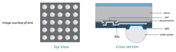
0.35µm Wafer-level bumping | |
|---|---|
Technology characteristics | Met. layer(s): 4 Thick Metal 4 Poly layer(s): 2, high resistive poly Maximum die size: 2cm x 2cm Usable cells: about 300 digital cells Available I/O: I/O cell library with digital pads is available 3V, 3V/5V, 5V with internal level shifters Floating digital pads available with 3.3V Temp. range: -40° C. / +125° C Supply voltage: 3.3V, 5V, 20V, 50V, 120V (max gate voltage 5V, 20V) |
Application area | Single die flip-chip packaging |
Design Kit version | Option supported by ams hitkit 4.10 ISR15, through an add-on |
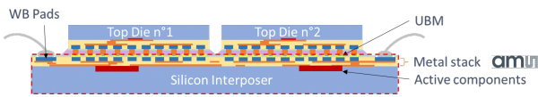
0.35µm Active Silicon Interposer with UBM | |
|---|---|
Technology characteristics | CMP, in partnership with ams, offers a 2.5D integration solution through specific MPW runs for silicon interposer production, allowing side by side integration of heterogeneous dies with higher interconnection densities than organic substrates, thus promoting package footprint reduction, increased inter-die bandwidth and decreased power consumption. This interposer offer is based on ams C35B4 metal stack (including 4 metal levels for routing), upon which a post-process is performed by an external subcontractor in order to produce a front-side Under Bump Metalization (or UBM) consisting of Ni/Pd/Au stack. For this active interposer offer, Active layers are available for CMOS integration, allowing the implementation of a wide range of functions to the interposer. The resulting interposer is ready to support flip-chip dies and is compatible with CMP OPEN 3D micro-bumps post-process offer (with a 50 µm min pitch). The interposer includes Wire-bonding pads to allow its connection to a PCB (as chip on board) or a compatible package. Note that this interposer is compatible with OPEN 3D TSV backside post-process. Access to this silicon interposer offer is based upon a formal DK request as well as administrative and partners approval through our web interface. Interposer run offer is available at any time. Guaranteed minimum delivered pieces: 40 ams CMOS C35 standard backend: 4 metal layers. Size limit for submitted design is 400 mm2. For design < 150 mm2, further cost reduction may be applicable under condition. |
Application area | Active Silicon Si-Interposer for 3D/2.5D integration |
Design Kit version | ams C35B4 4.10 ISR15 |
Libraries | ams C35B4 libraries |
Turnaround time | 23 weeks |

Passive Silicon Interposer with UBM | |
|---|---|
Technology characteristics | CIME-P and Fraunhofer IIS, in partnership with ams OSRAM, offer a 2.5D integration solution through specific MPW runs for silicon interposer production, allowing side by side integration of heterogeneous dies with higher interconnection densities than organic substrates, thus promoting package footprint reduction, increased inter-die bandwidth and decreased power consumption. This interposer offer is based on ams C35B4 metal stack (including 4 metal levels for routing), upon which a post-process is performed by an external subcontractor in order to produce a front-side Under Bump Metalization (or UBM) consisting of Ni/Pd/Au stack. For this passive interposer offer, only the backend is processed (no active component available), for high density routing applications and passive component integration. The resulting interposer is ready to support flip-chip dies and is compatible with CMP OPEN 3D micro-bumps post-process offer (with a 50 µm min pitch). The interposer includes Wire-bonding pads to allow its connection to a PCB (as chip on board) or a compatible package. Note that this interposer is compatible with OPEN 3D TSV backside post-process. Access to this silicon interposer offer is based upon a formal DK request as well as administrative and partners approval through our web interface. Interposer run offer is available at any time. Guaranteed minimum delivered pieces: 40 ams CMOS C35 standard backend: 4 metal layers. Size limit for submitted design is 400 mm2. For design < 150 mm2, further cost reduction may be applicable under condition. |
Application area | Passive Silicon Si-Interposer for 3D/2.5D integration |
Design Kit version | ams C35B4 4.10 ISR15 |
Libraries | ams C35B4 libraries |
Turnaround time | 23 weeks |
MEMS Backside Bulk Micromachining | |
|---|---|
Technology characteristics | ams 0.35µ processes 4LM + Post Process On-chip suspended membrane with piezoresistors. |
Special Features | 0.35 µm CMOS post process from ams + TMAH (Tetra Methyl Ammonium Hydroxide) post process etching ; No additional mask for the MEMS post process |
Design Kit version | ams C35B4 4.10 ISR15 |
Libraries | ams C35B4 libraries |
Turnaround time | Typical leadtime: 14-16 weeks from MPW run deadline to packaged parts |
MEMS Frontside Bulk Micromachining | |
|---|---|
Technology characteristics | ams 0.35µ processes Process cross section Thick Metal module instead of Metal 4 module and with MIM capacitor module Poly layer(s): 2, high resistive poly Maximum die size: 2cm x 2cm DLP Usable cells: about 300 digital cells Available I/O: I/O cell library with digital pads is available 3.3V, 3V/5V, 5V with internal level shifters Temp. range: -40° C. / +125° C Supply voltage: 5V or 3.3V Die size: Minimum charge of 3 mm². |
Special features | 0.35 µm CMOS post process from ams + TMAH (Tetra Methyl Ammonium Hydroxide) post process etching ; No additional mask for the MEMS post process |
Application area | MEMS, micromechanics, MOEMS |
Design Kit version | ams C35B4 4.10 ISR15 |
Libraries | ams C35B4 libraries |
Turnaround time | Typical leadtime: 14-16 weeks from MPW run deadline to to packaged parts |