Europractice users can get access to EM Microelectronic’s 0.11µm ALP11 Logic 3v3 technology.
EM Microelectronic 0.11µm ALP11 Logic 3v3 | |
|---|---|
Technology characteristics | Met. layers: 5 / 6. Minimum Gate length: 120nm [drawn] Dual Gate Oxides: ThinGOX [1.50V typ] and DualGOX [3.30V typ] FEOL isolation: Non Epi or p-Epi substrate, STI [Shallow trench isolation] Typical Supply voltage: 1.5V & 3.3V |
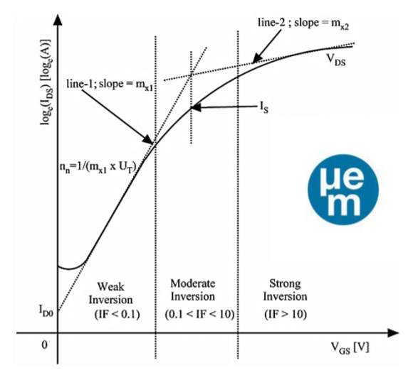
Special features | EKV models with parameters for near/sub Vth operations Digital cell library optimized for Low Power/Low Voltage I/O pads library with low leakage ESD protections |
Application area | Ultra-Low Power, Ultra-Low Voltage Analog Designs (low leakage, low noise, pairing) Mixed signal (250kGates/mm2) Low current (nA bias), Low voltage (down to 0.4V) |
Design kits version | 1.5 (Feb-2026) |
Frontend Backend tools | Cadence IC 25.1 |
Simulation tools | Spectre (Cadence) Primesim XA (Synopsys) |
Verification tools | PVS (Cadence) |
Parasitics extraction tools | Quantus (Cadence) |
Place route tools | Innovus (Cadence) or Fusion Compiler (Synopsys) |
Turnaround Time | 12-15 weeks from MPW run deadline to packaged parts |