Europractice provides access to the Pathfinding PDKs (P-PDK) developed within the NanoIC pilot line. Hosted by imec and supported by pan-European partnerships, the NanoIC pilot line boosts the development and commercialization of beyond-2nm systems-on-chip. The purpose of the P-PDKs is to facilitate the creation of virtual digital designs in advanced CMOS technologies for 2nm and beyond.
NanoIC Logic P-PDKs endeavour to bridge the gap between design and technology communities. Built on the imec Logic roadmap, these PDKs contain a library of electrically characterized logic standard (std) cells with layout compliant to lithography defined design rules. The electrical performance of the library is obtained from circuit simulations using in-house developed models for devices and interconnects. These models are themselves based on process and TCAD simulations calibrated with silicon data.
The imec N2 Digital CMOS kit is based on the imec N2 technology node process assumptions. It features gate-all-around nanosheet devices and provides the flexibility of a Front-Side and a backside PDN. It contains a library of 102 electrically characterized logic standard (std) cells.
The logic library is built around a 6 track standard cell architecture and the devices contain a stack of 4 nanosheets.
In terms of ground rules, the gate pitch (CPP) is 48nm and the minimum metal pitch (MP) is 22nm. The backside PDN library contains built-in power connections through nano-TSVs to the backside power rails.
Items | Parameters |
|---|---|
CPP | 48 nm |
Gate length | 15 nm |
SDC height | 132nm |
SDC in library | 102 |
Total routing metal layers | 17 |
Frontside metal layers | 13 |
Backside metal layers | 4 |
Device flavours | 4 (ulvt, lvt, svt, and hvt) |
Vdd Characterization | 0.5 V, 0.7 V, and 0.9 V |
Backside connection | TSVM (Through Silicon Via to the side of the device) |
Memory | 29 SRAM Macro |
The virtual P-PDK contains the necessary infrastructure and design kits for digital design including:
PDK | Folder / File | File Description |
|---|---|---|
Instructions | Readme.txt | PDK overview & setup instruction |
Installation script | BIN | Install PDK setup file |
Verification/validation decks | CALIBRE | DRC, LVS |
Symbolic view for schematics | PDKTECH | Device symbol (not parametrized), Technology.tf, Display.drf, Layer Map |
Device compact models | MODEL | Spice and Spectre modelcard |
Tools setups (Cadence, Calibre) | TOOLS | cds.lib, cds.init and setup files |
Documentation | DOC | PDF Documents for DRM, Compact model and User guide |
The A14 P-PDK is based on projected performance of the technology developed in the imec NanoIC pilot line and supports early Design-Technology Co-Optimization (DTCO) to give guidance on process assumptions and design rules. It enables early design assessments in advanced technologies, bridging the gap between technology and design communities from academia and industry. It is thus a vehicle to access the NanoIC pilot line capabilities and knowledge, helping generation of IPs in advanced nodes in Europe and training of the design community.
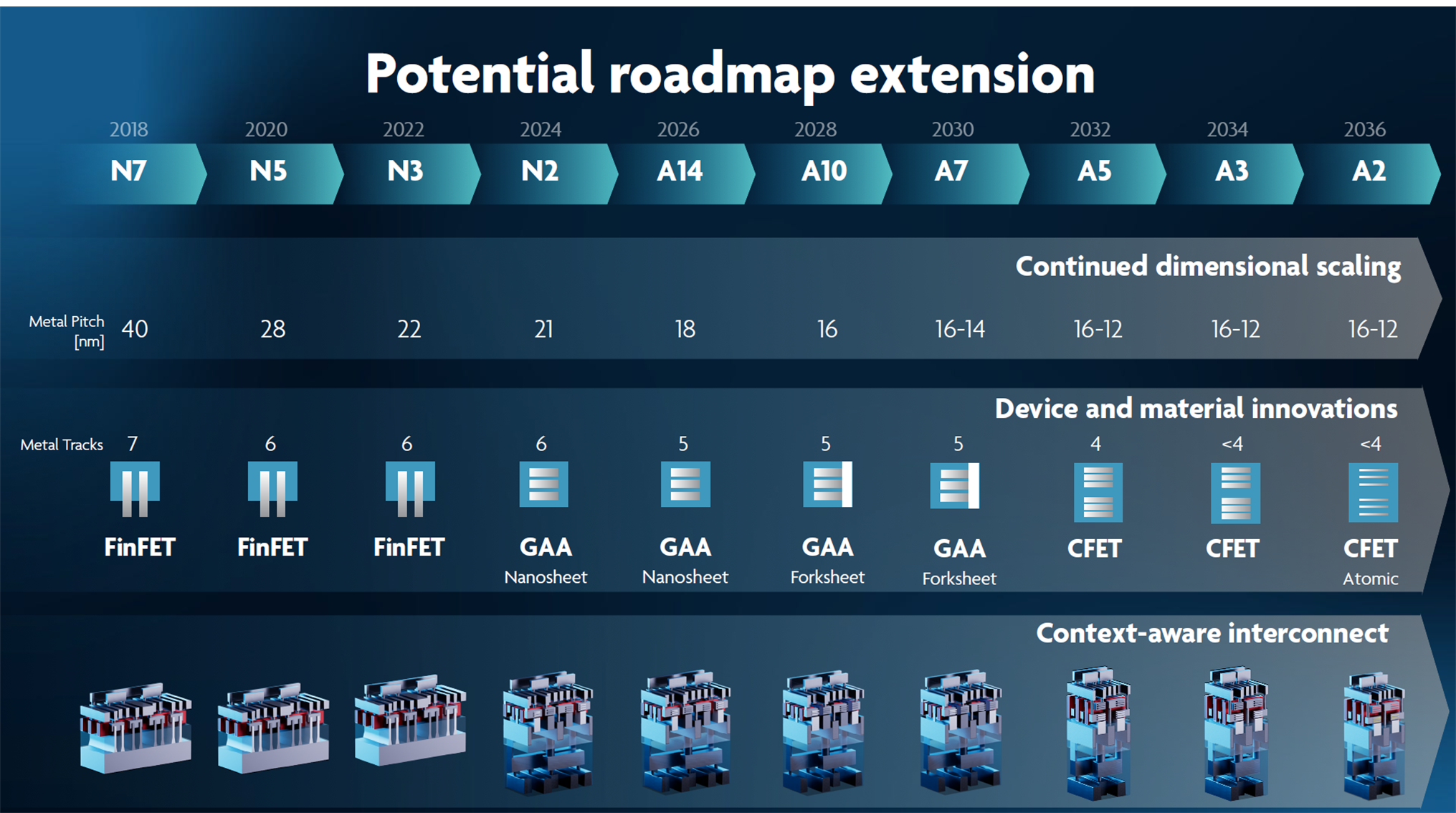
Compared to N2, the A14 technology differ mainly by the contacting scheme to connect the backside metals to the devices: while N2 used TSVM, A14 assumes direct Backside contact (BCT) to the source/drain EPI from the BSPDN as technology booster. This leads to a more compact structure with smaller silicon footprint. This evolution in contacting scheme reflects the roadmap foreseen in backside enablement shown in Figure 1, with increasing processing complexity but also performance.
Items | Parameters |
|---|---|
CPP | 45 nm |
Gate length | 15 nm |
SDC height | 115 nm |
SDC in library | 162 |
Total routing metal layers | 18 |
Frontside metal layers | 13 |
Backside metal layers | 5 |
Device flavours | 4 (ulvt, lvt, svt, and hvt) |
Area gains Vs N2 | ~18% |
Power gain vs N2 at iso frequency | ~7% |
Vdd Characterization | 0.5 V, 0.7 V, and 0.9 V |
Backside connection | BCT (Backside direct contact to device) |
The virtual P-PDK contains the necessary infrastructure and design kits for digital design including:
PDK | Folder / File | File Description |
|---|---|---|
Instructions | Readme.txt | PDK overview & setup instruction |
Installation script | BIN | Install PDK setup file |
Verification/validation decks | CALIBRE | DRC, LVS |
Symbolic view for schematics | PDKTECH | Device symbol (not parametrized), Technology.tf, Display.drf, Layer Map |
Device compact models | MODEL | Spice and Spectre modelcard |
Tools setups (Cadence, Calibre) | TOOLS | cds.lib, cds.init and setup files |
Documentation | DOC | PDF Documents for DRM, Compact model and User guide |
The imec IGZO-based eDRAM Technology PDK is based on IMEC’s roadmap and experimental results associated with its IGZO-based, BEOL-embedded eDRAM Technology. This version enables design at simulation level of application-specific novel memory concepts, based on models calibrated on the best available IGZO device experimental data. It allows the combination of eDRAM device models and BEOL-embedded bitcells with third-party CMOS frontend technologies (the latter needs to be provided by the user through a suitable PDK installation).
The imec IGZO-based eDRAM Technology PDK aims at providing the user with tools and models enabling universities, startups, industry players in the EU ecosystem to explore a multitude of application-specific, novel memory concepts for eDRAM architectures at a simulation level.
This PDK contains models of selected IGZO eDRAM bitcell architectures, selected on the base of early Design-Technology Co-Optimization (DTCO) efforts, complemented with the extracted parasitism associated with specific physical implementations designed under the assumption of N40 or N7 technology rules.
The IMEC IGZO-based eDRAM Technology PDK v0.0 contains:
The Die-to-Wafer hybrid bonding (IC1 D2W) P-PDK from imec brings a new level of high-density chip-to-chip integration, enabling ultra‑dense die‑to‑die 3D connections.
D2W hybrid bonding enables high-density integration by providing extremely compact, direct connections between dies in the third dimension. Instead of relying on traditional copper bumps, hybrid bonding forms direct oxide-to-oxide links between the CMOS die and the package interface. This eliminates the parasitic effects associated with copper bumping and enables low-loss, energy-efficient communication pathways.
The PDK provides designers with access to highly dense die-to-die 3D connections, early process assumptions, design rules, and wafer-level packaging insights. This supports the development of next-generation advanced packaging designs in Europe and helps train the design community.
Items | Parameters |
|---|---|
Scaled pitch die to wafer (hybrid bonding) | available, 2µm pad pitch |
Width, space of metal line (M1) | 0.5µm, 0.5µm |
Width, space of via (VIA) | min 0.4µm / max 0.6µm, 0.4µm |
Width, space of metal line (M2) | 0.3µm, 0.5µm |
The P-PDK contains the necessary infrastructure and design kits for advanced interconnect design, including:
The Fine-Pitch Redistribution Layer (IC2 RDL) P-PDK from imec brings a new level of high-density chip-to-chip integration, enabling RDL line widths and spaces down to 1.3 microns and micro-bump pitches as tight as 20 microns on advanced polymer-based substrates.
The IC2 RDL PDK provides designers with early access to high-density polymer-based die-to-die interconnects, including process assumptions, design rules, and wafer-level packaging insights. It supports the development of advanced packaging designs in Europe and helps train the design community.
Items | Parameters |
|---|---|
Micro bump pitch | 20µm |
Width, space of RDL | 1.3µm, 1.3µm |
Width, space of via (VIA) | 1.3µm, 1.3µm |
The P-PDK contains the necessary infrastructure and design kits for advanced interconnect design, including: