The 2D Experimental Pilot Line (2D-EPL) has launched its third multi-project wafer (MPW) run where universities, research institutes and companies can include their designs as dies on joint wafers. The 2D-EPL’s third MPW run is mainly intended towards electronics but can also include sensor devices (e.g. Hall sensor, but via opening on graphene is not in the scope of this run) and will be provided by AMO GmbH. The design of the device can be adjusted within the specifications.
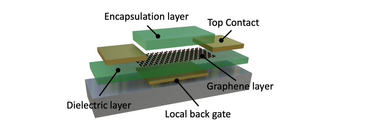
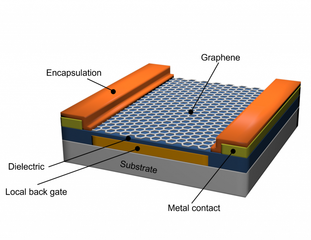
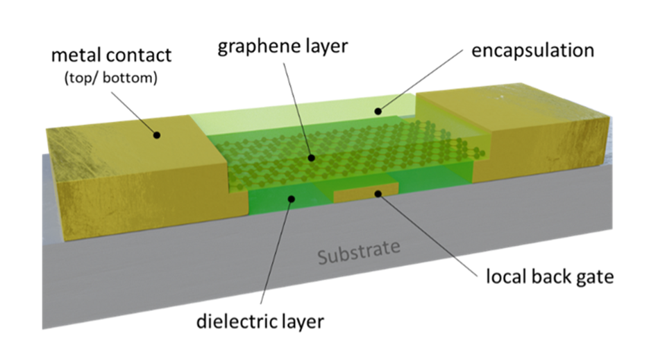
The offered device structure is a GFET consisting of the following fabrication steps:
Back gate
Dielectric deposition & vias opening
Fabrication of adhesion pads
Wafer scale graphene transfer & patterning
Top contacts fabrication
Encapsulation & vias opening (not on top of graphene)
About AMO
Located in Aachen, Germany, close to the borders of Belgium and the Netherlands, the research foundry AMO GmbH, a non-profit nanotechnology SME, follows the mission to efficiently close the gap between university research and industrial application. It demonstrates innovative technologies and introduces new materials, including their implementation in novel device architectures, prototyping and small volume fabrication. A state-of-the-art 400 m² cleanroom is operated and a range of services from consulting to prototype development is offered. In recent years, AMO has become a global player in 2D materials research for electronics and photonics.
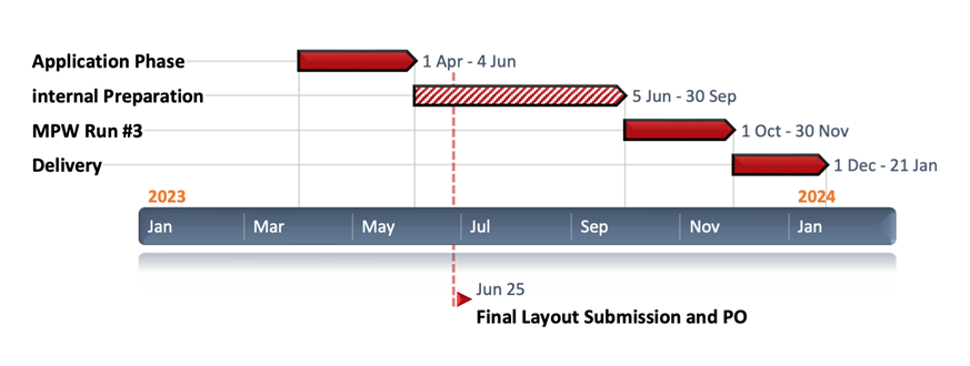
Important Dates
25 June: Final Layout Submission must be done and PO received.
December 2023: The chips are expected to be delivered.
PRICING
1300€ set price for four dies with identical design (1×1 cm²)
250€ for each additional die with identical design
Scheme with the different layers of the final GFET structure:
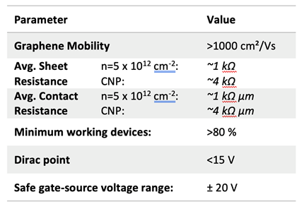
Technology Characteristics
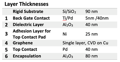
Substrate
Material: Silicon
Basic die size: 1 x 1 cm²
Resolution
General design rule: 10µm for in-layer critical dimension and over-layer alignment
Characterization
Raman characterisation
Electrical measurements for as-fabricated reference devices
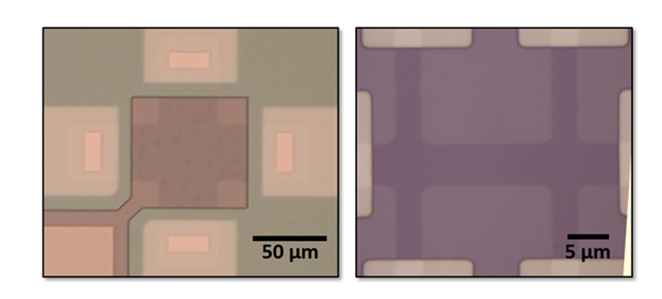
General optical inspection of your devices
Application
Bio/ Gas/ Chemical sensors, Hall Sensors, Photodetectors
The schematic shows the offered baseline process with top/bottom contact and local gate option.
Europractice and 2D-EPL webinars on Graphene
Manage Consent
We use cookies to optimize our website and our service.
Functional
Always active
The technical storage or access is strictly necessary for the legitimate purpose of enabling the use of a specific service explicitly requested by the subscriber or user, or for the sole purpose of carrying out the transmission of a communication over an electronic communications network.
Preferences
The technical storage or access is necessary for the legitimate purpose of storing preferences that are not requested by the subscriber or user.
Statistics
The technical storage or access that is used exclusively for statistical purposes.The technical storage or access that is used exclusively for anonymous statistical purposes. Without a subpoena, voluntary compliance on the part of your Internet Service Provider, or additional records from a third party, information stored or retrieved for this purpose alone cannot usually be used to identify you.
Marketing
The technical storage or access is required to create user profiles to send advertising, or to track the user on a website or across several websites for similar marketing purposes.