Flexible integrated circuits (FlexICs) enable novel solutions that are simply not possible with conventional electronics. Particularly suited to applications where form factor and cost outweigh speed and performance criteria, FlexICs excel in areas such as radio frequency identification (RFID), multiplexing, driver and readout circuitry, and basic computation.
Fab description
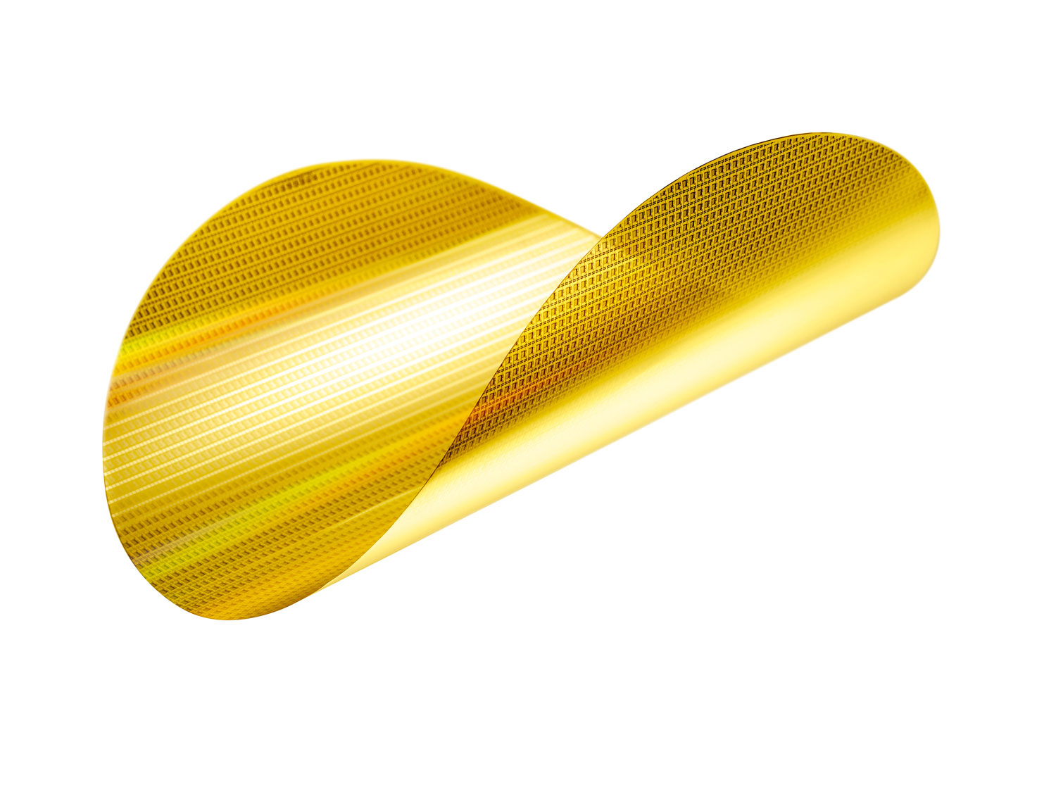
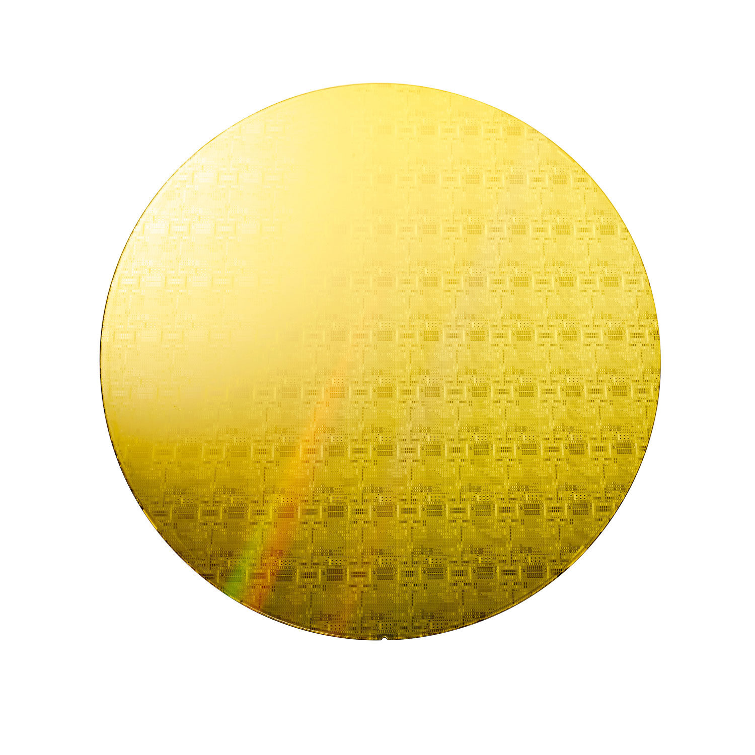
Pragmatic Semiconductor is pioneering flexible semiconductor technology to sustainably bridge digital and physical worlds. Driven by optimised, purpose-led design, FlexICs – ultra-thin, flexible chips – empower innovators with connect, sense and compute capabilities to deliver edge and item-level intelligence at scale.
Using thin-film transistor (TFT) technology in combination with conventional semiconductor processing equipment, Pragmatic Semiconductor’s FlexIC Foundry service takes FlexICs from tape-out to delivery in just weeks, enabling agile iterations, early end-user testing, and an accelerated time to market – at a fraction of the cost of silicon.
Pragmatic Semiconductor’s innovative manufacturing process uses fewer steps than silicon semiconductor fabrication, at lower temperatures. This results in significantly reduced energy and water consumption, fewer harmful chemicals, and a carbon footprint that is orders of magnitude smaller.
Platform Gen 3 offers a 600 nm minimum channel dimension n-type FET, a dedicated 200 kΩ/sq resistor layer and 4.5 fF/μm2 metal-insulator-metal capacitors. Four metal layers provide efficient routing and interconnects, with a 4 μm routing pitch. The technology is packaged with passivation for protection and isolation, and a redistribution layer (RDL) with aluminium metallisation for compatible attachment methods.