![]()
About United Monolithic Semiconductors (UMS)
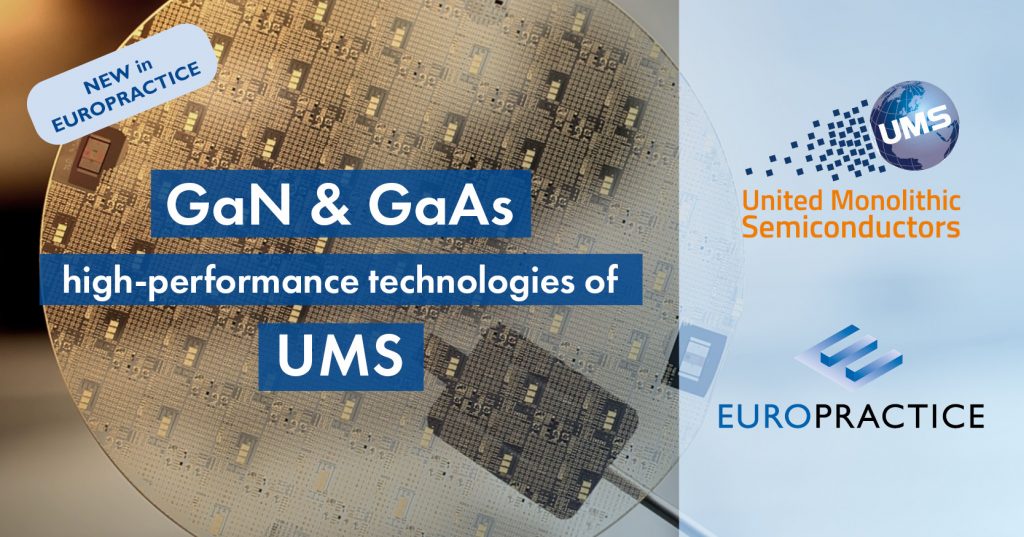
United Monolithic Semiconductors (UMS) is the European leader in offering RF MMIC products and foundry services for specialized markets, including Defence and Space, telecommunications, automotive radar and industrial sensors, with major locations in both France and Germany.
UMS in-house GaAs and GaN processes provide the technology platform to allow the design of our leading edge products and form the basis of our foundry service offer to external design centers.
Continuous and customer led innovation is at the heart of UMS’ continuing success. UMS has strong relationships with many of the major R&D centers and Universities throughout Europe, actively participating in many advanced and collaborative developments to create the technologies and products needed for future markets.
www.ums-rf.com

About Europractice
Europractice is a consortium of research organisations that provides European industry and academia with a platform to develop electronic circuits and systems. For nearly 30 years, the consortium has offered affordable access to prototyping and volume production services in a wide range of technologies, including ASICs, MEMS, Photonics and more. For future generations of engineers, Europractice has provided design tools and a broad training offer ensuring the growing digital economy in Europe. The consortium consists of five partners, namely imec (Belgium), UKRI-STFC (UK), Fraunhofer IIS (Germany), CIME-P from Grenoble INP (France) and Tyndall National Institute (Ireland). Over the years, Europractice has been supported by the European Commission, which allowed expansion into new markets and continuation of the high-quality service to more than 600 academic institutions and over 300 SMEs.

About Fraunhofer IIS
The Fraunhofer Institute for Integrated Circuits IIS, headquartered in Erlangen, Germany, conducts world-class research on microelectronic and IT system solutions and services. Today, it is the largest institute of the Fraunhofer-Gesellschaft.
With more than 30 years of experience in professional IC-Design, Fraunhofer IIS is development partner for customized solutions. Focus is on mixed-signal ASIC and SoC design for industrial, communication, consumer and automotive applications as well as on integrated solutions for increasingly complex electronic systems.
Fraunhofer IIS is partner of ams-OSRAM, Fraunhofer IISB, GLOBALFOUNDRIES, IHP, UMS and X-Fab providing turnkey solutions for technologies from CMOS, HV-CMOS, SiGe, SiC, GaN, GaAs down to 22 FDSOI and 12 nm FinFET.
www.iis.fraunhofer.de