Europractice provides access to SINTEF’s state-of-the-art thin film piezoelectric MEMS using high-quality PZT as the piezoelectric layer. Europractice users can get from 3 up to 12 6-inch wafers of piezoMEMS devices per Multi-Project Batch (MPB) scheme, each accommodating various designs and test structures. Each process offers high reliability and has an extensive portfolio of demonstrated applications and use cases with academia as well as industry.
Imec (Leuven, Belgium) is the service center for SINTEF’s piezoMEMS technologies within Europractice, providing customers support and access to this technology.
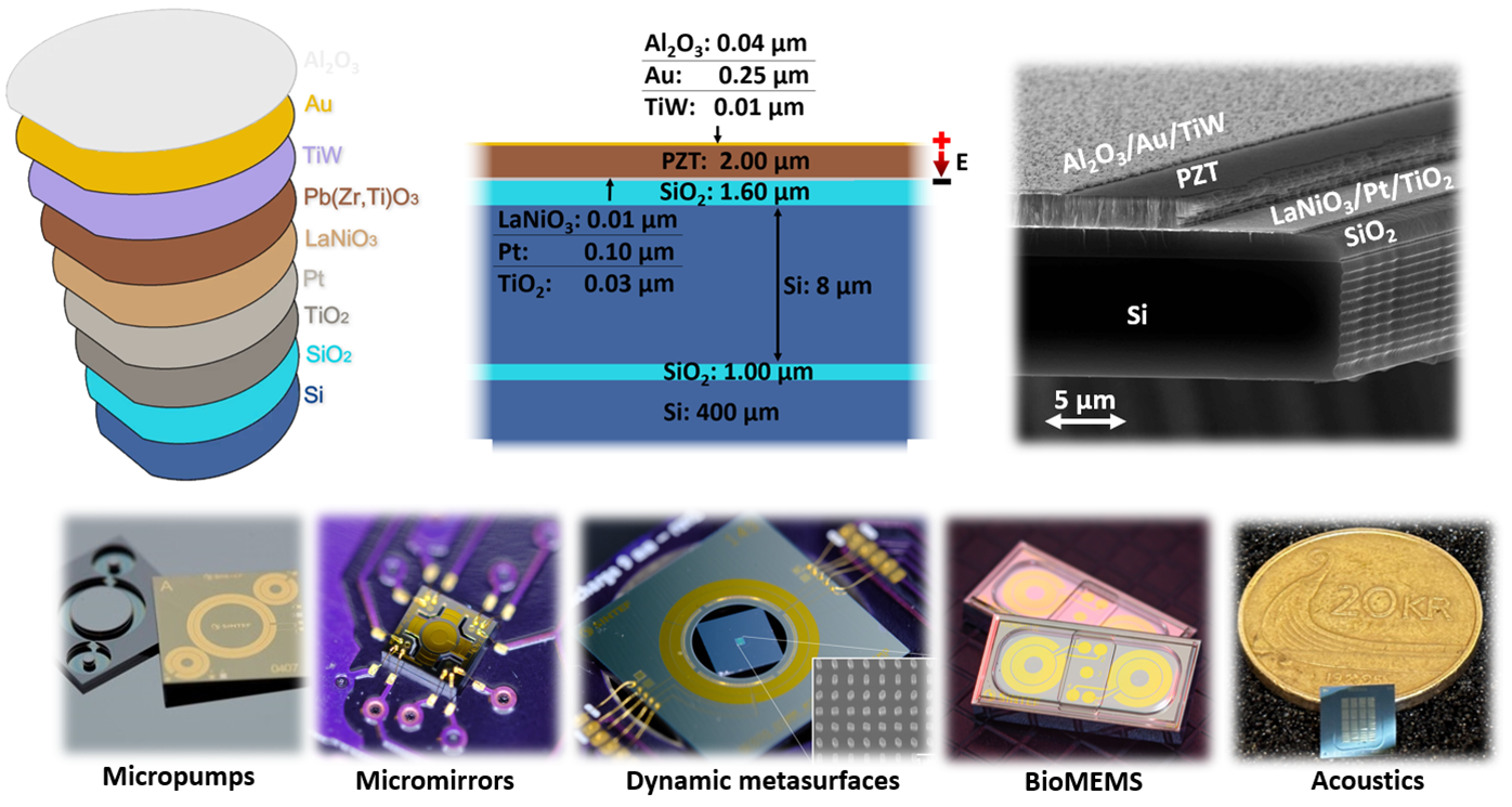
A typical piezoMEMS process is shown in the table below.
SINTEF MEMS | |
|---|---|
Typical technology characteristics | Typical Si substrate: • Type: SOI , DSP • Size: 6-inch (150 mm) • Thickness: 400 µm • Dopant: Phosphorous/Boron • Orientation: <100> • Resistivity: 1-10 Ωcm • Device layer: 8 µm Top electrode: • Material: Au • Thickness: 250 nm • Adhesion: TiW Piezoelectric layer: • Composition: Nb doped Pb(Zr,Ti)O3 • Thickness: 2 µm • Deposition: CSD Bottom electrode: • Material: Pt <111>, LaNiO3 <100> • Thickness: 100 nm / 15 nm |
Special features | High piezoelectric response High uniformity Low in-plane stress High breakdown strength Low power-consumption High electrical reliability and low fatigue Robust in harsh ambient: Space-qualified by ESA 2021 High device precision and repeatability |
Selected application areas | Micromirrors and optics[1]: • Tunable metasurfaces[2] • Focusing lenses[3] • Compact interferometers, ex. Fabry-Perot, Michelson[4] • Scanners, projectors and 3D cameras[5] Sensors and actuators: • BioMEMS and biosensors[6] • Gas-detection[7] • Ultrasound[8] • Space-applications[9] • RF and THz MEMS |
[1] www.sintef.no/en/sintef-research-areas/sensors/small-mirrors-major-advances/
[2] C. Meng et al., “Dynamic piezoelectric MEMS-based optical metasurfaces,” Sci Adv, vol. 7, no. 26, p. eabg5639, 2021, doi: 10.1126/sciadv.abg5639.
[3] F. Dullo, J. Jose, G. Bouquet, Z. Skokic, and C. Dirdal, “Metasurface lens that is converging or diverging depending on transmission direction enables ultra-compact MEMS tunable reflective lens,” 2024. [Online]. Available: https://arxiv.org/abs/2402.02755
[4] T. Bakke, A. Vogl, O. Żero, F. Tyholdt, I.-R. Johansen, and D. Wang, “A novel ultra-planar, long-stroke and low-voltage piezoelectric micromirror,” Journal of Micromechanics and Microengineering, vol. 20, p. 064010, 2010, doi: 10.1088/0960-1317/20/6/064010.
[5] J. Thorstensen, J. T. Thielemann, P. Risholm, J. Gjessing, R. Dahl-Hansen, and J. Tschudi, “High-quality dense 3D point clouds with active stereo and a miniaturizable interferometric pattern projector,” Opt. Express, vol. 29, no. 25, pp. 41081–41097, 2021, doi: 10.1364/OE.444641.
[6] www.sintef.no/en/expertise/digital/microsystems-and-nanotechnology/biomems/
[7] “Tunable – Sense of Smell. Artificially Perfected.,” www.tunable.com/
[8] www.sonair.com/
[9] R. Dahl-Hansen, J. Gjessing, P. Mardilovich, C. Fragkiadakis, and J. Thorstensen, “Reliable Pb(Zr,Ti)O3-based thin film piezoelectric micromirrors for space-applications,” Appl Phys Lett, vol. 121, no. 13, Sep. 2022, doi: 10.1063/5.0106933.