Europractice partner Tyndall offers two variants of piezoMEMS stack with AlScN (Scandium 6.5 atomic percentage) as the piezoelectric layer, that can be used for the development of piezo based devices for a variety of applications.
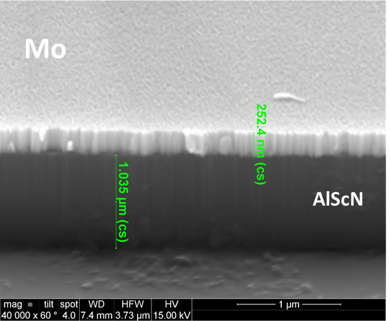
The single electrode stack has a silicon substrate with an optional TOX (Thermal Oxide) layer, a Piezoelectric layer of AlScN and Molybdenum as the top electrode. This stack could further be used by any researcher / industry with in-house microfabrication capabilities to carry out post processing at their facility.
Piezoelectric Layer of AlScN with D33 around 6 pC/N (As measured by Piezometer PM300)
Application area
PiezoMEMS sensors and actuators Energy Harvesting Ultrasonic transducers Medical applications Optics RF applications Biosensors Quantum physics applications Space applications etc.
Pictorial representation of the single electrode layer stack
SEM image of the single electrode layer stack
Dual electrode layer stack
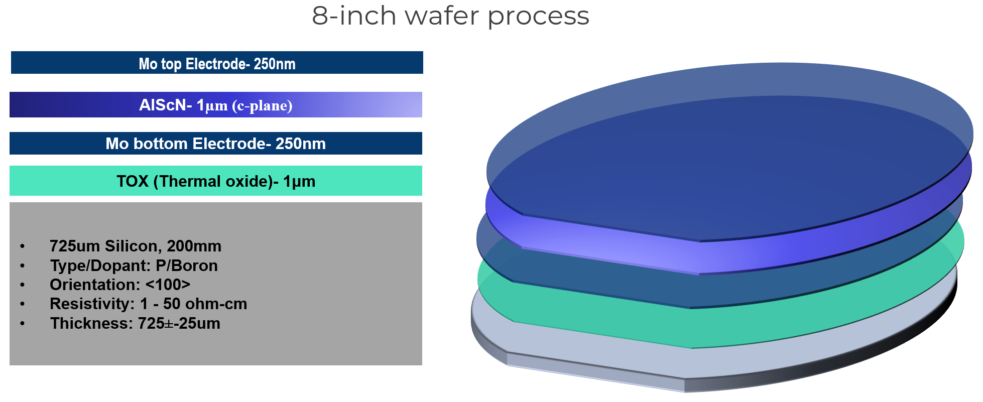
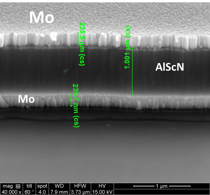
The dual electrode layer stack has a silicon substrate with TOX (Thermal oxide) layer, a bottom Molybdenum metal electrode, the Piezoelectric layer of AlScN and a Molybdenum top electrode. This stack could further be used by any researcher / industry with in-house microfabrication capabilities to carry out post processing at their facility.
Piezoelectric Layer of AlScN with D33 around 6pC/N (As measured by Piezometer PM300)
Application area
PiezoMEMS sensors and actuators Energy Harvesting Ultrasonic transducers Medical applications Optics RF applications Biosensors Quantum physics applications Space applications etc.
Pictorial representation of the dual electrode layer stack
SEM image of the dual electrode layer stack
Manage Consent
We use cookies to optimize our website and our service.
Functional
Always active
The technical storage or access is strictly necessary for the legitimate purpose of enabling the use of a specific service explicitly requested by the subscriber or user, or for the sole purpose of carrying out the transmission of a communication over an electronic communications network.
Preferences
The technical storage or access is necessary for the legitimate purpose of storing preferences that are not requested by the subscriber or user.
Statistics
The technical storage or access that is used exclusively for statistical purposes.The technical storage or access that is used exclusively for anonymous statistical purposes. Without a subpoena, voluntary compliance on the part of your Internet Service Provider, or additional records from a third party, information stored or retrieved for this purpose alone cannot usually be used to identify you.
Marketing
The technical storage or access is required to create user profiles to send advertising, or to track the user on a website or across several websites for similar marketing purposes.