CEA-Leti’s LUMIK optomechanical sensor technology represents the next evolution of Micro Electro Mechanical Sensors (MEMS) sensors. From the capacitive sensors of the 1980s to the more recent piezoresistive sensors, MEMS have become increasingly sensitive over the past several decades. Today, CEA-Leti is bringing silicon photonics to high-performance MEMS for a new generation of optomechanical sensors.
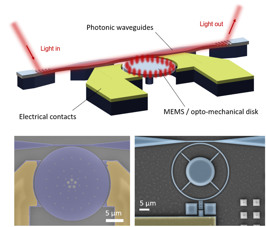
LUMIK is a technology combining silicon photonics and MEMS components in silicon-on-insulator substrates. Selective doping and metallic contacts allow electrical actuation and highly-performant opto-mechanical detection.
CEA-Leti LUMIK | |
|---|---|
Technology characteristics | Silicon-On-Insulator (SOI) substrate Wafer size: 200mm (725 µm thick) Top silicon layer: • Resistivity: 8.5-11.5 Ω.cm • Crystal orientation: <100> • Doping type: P/Boron Buried oxide thickness: 1µm Definition of grating couplers using DUV lithography followed by partial Si dry etching (depth of 70nm). Definition of photonic and mechanical components using e-beam lithography and Si dry etching (220 nm). Definition of electrodes via localized p-doping in Si (5×10¹⁹ at/cm³) combined with one metal level: AlSi electrical lines. Structures’ release by HF etching Die dicing by stealth dicing Design area – multiples of 4 x 4 mm² |
Special features | Optomechanical process: combining mechanical, electrical and photonic components Optimized for 1550 nm telecom wavelengths Optical interconnections through grating couplers Electrical interconnections / pads with AlSi contacts |
Application areas | MEMS sensors with extreme sensitivity and bandwidth / speed Example application areas: • Biological sensing • Silicon clocks • Mass spectrometry • Particle sensing • Inertial |
Turnaround time | Around 10 months for manufacturing 1 additional month for dicing and bare dies delivery |
CEA-Leti’s optomechanical resonators have already surpassed MEMS in several sensing applications, enabling breakthroughs such as video-rate atomic force microscopy, ultra-sensitive mass detection of non-spherical particles, GHz MEMS clocks and GHz Brownian motion detection in liquids.
[1] F.-R. Lamberti et al., “Real-Time Sensing with Multiplexed Optomechanical Resonators,” Nano Lett., Feb. 2022, doi: 10.1021/acs.nanolett.1c04017.
[2] M. Sansa et al., “Optomechanical mass spectrometry,” Nature Communications, vol. 11, no. 1, Art. no. 1, Jul. 2020, doi: 10.1038/s41467-020-17592-9.
[3] T. Furcatte et al., “Towards GHz low phase noise oscillators with electro-optomechanical resonators,” in 2024 IEEE Ultrasonics, Ferroelectrics, and Frequency Control Joint Symposium (UFFC-JS), Sep. 2024, pp. 1–4. doi: 10.1109/UFFC-JS60046.2024.10793753.
[4] A. Marković et al., “Suspended tip overhanging from chip edge for atomic force microscopy with an optomechanical resonator,” JOM, vol. 4, no. 3, p. 033501, Sep. 2024, doi: 10.1117/1.JOM.4.3.033501.