Europractice customers can access the following technologies of Science (former MEMSCAP).

Europractice customers can access the following technologies of Science (former MEMSCAP).
Science PolyTM is the industry’s longest-running MEMS multi-project wafer service, with over a decade of history. Many universities use the service today as a way to teach beginning MEMS design at the undergraduate level, using Science Poly as the “example” process.
Science PolyTM is a three-layer polysilicon surface and bulk micromachining process, with 2 sacrificial layers and one metal layer. Eight mask levels create 7 physical layers. The minimum feature size in Science Poly is 2µm.
Science Poly | |
|---|---|
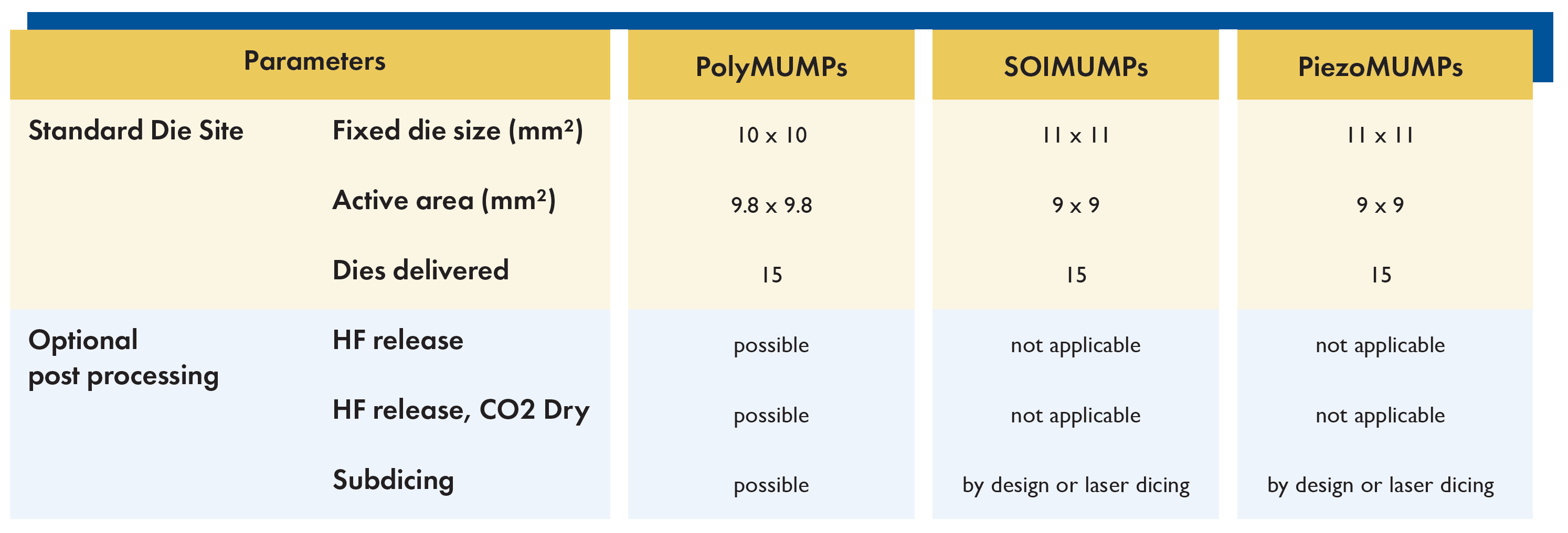
Technology characteristics | Active area (mm2): 9.8 x 9.8 Polysilicon/ gold Surface micromachining |
Special features
| Polysilicon Surface Micomachining. One poly ground layer, two structural poly layers, one gold metal layer, two oxide release layers. |
Application area
| MEMS, micromechanics, MOEMS
|
Science SOITM uses a SOI wafer with a thickness of 10µm or 25µm and allows the designer to pattern and etch both sides of the SOI wafer down to the buried oxide, enabling through-holes to pass light through. Two metal layers, one for bond pads and one for reflectivity, are included in the Standard Process. The minimum feature size in Science SOITM is 2µm.
Science SOI | |
|---|---|
Technology characteristics | Active area (mm2): 9 x 9
|
Special features
| DRIE (Deep Reactive Ion Etching) on Silicon-On-Insulator wafer
|
Application area
| MEMS, micromechanics, MOEMS
|
The Science PiezoTM process is based on the SOIMUMPs process with 10µm SOI thickness. Its distinguishing feature is a piezoelectric layer of AlN. Top-contact to the piezoelectric layer and the SOI is enabled by means of a patterned layer of Metal. Patterning of the oxide layer that separates the SOI and the AlN allows for contact between the latter. Patterning of the SOI and openings in the handle silicon are available as is the case for Science PiezoTM.
Science Piezo | |
|---|---|
Technology characteristics | Active area (mm2): 9 x 9
|
Special features
| DRIE (Deep Reactive Ion Etching) on Silicon-On-Insulator wafer + piezoelectric layer
|
Application area
| MEMS, micromechanics, MOEMS
|