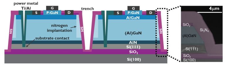
Technology Characteristics | In this technology, a GaN layer is epitaxially grown on a 200mm SOI wafer (Si(100)/SiO2/Si(111)) using metal-organic chemical vapor deposition (MOCVD). The stack consists of an AlN nucleation layer, an (Al)GaN buffer layer, a GaN channel layer, an AlGaN barrier layer and a Mg-doped p-GaN layer. Delicate strain engineering is performed to control the stress built up in the wafer during growth, resulting in a GaN-on-SOI wafer with controlled warpage and good mechanical strength. Furthermore, e-mode p-GaN HEMTs can be processed and TiN/p-GaN stacks used for the gates. |
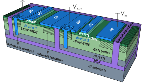
| – Integrate multiple transistors on a single IC using trench isolation.
– Save package cost by packaging one instead of multiple devices
– Reduce system parasitic inductance.
To use the full potential of the fast switching speed of GaN power devices, the drivers should be co-integrated to lower the parasitic inductance.
Further functionality can be added through the low-voltage logic and analog switches, the high-ohmic and low-ohmic resistors and the integrated MIM-capacitors. |
| High power switching and power conversion: 100V and 650V
|
| v.1.4.2 at 100V
v.2.2.3 at 650V
|
| |
| |
| The PDK includes process documentation, library devices, layout guidelines for custom design, verification and models.
– Low-ohmic and high-ohmic resistors
– Metal/oxide/metal capacitors
– Low voltage logic devices
– Metal/insulator/metal |
| Approximately 26 weeks since MPW submission deadline, it includes already 6 weeks of DRC iterations |
| Until Cu/Ni/Au RDL for wire-bonding or until CuRDL/CuPillars to mount directly on PCB. |