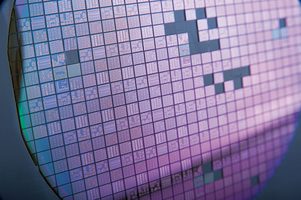
Fraunhofer IISB offers early-access to its 2µm SiC CMOS technology including NMOS and PMOS transistors as well as passive components and pn-diodes for integrated circuits. These circuits are capable of operating at temperatures above 300 °C (up to approx. 600 °C). Additional process modules are available for high-voltage devices, isolated transistors and SiC device templates exceeding CMOS circuits.
The targeted applications for this technology include integrated circuits beyond silicon for extremely harsh environments including high temperatures and radiation levels with low leakage. Additionally, the technology can be tailored to obtain specialized optical SiC devices and quantum sensor templates.
The double well 2 µm SiC CMOS process consists of 1 Poly and 2 Metal (Pt) layers and includes dedicated ohmic contacts to p+– and n+-doped SiC regions. A thick gate oxide allows peak voltages up to 20 V, and additional dielectric isolation is provided through an active area layer using a field oxide.
The standard process flow for this planar technology includes these process modules:
Module | Description | |
|---|---|---|
Alignment marks and scribe | Dry etching of the alignment marks for lithography | |
Implantation | pwell
| • Implantation of N and Al • Masking: Photoresist or oxide (depending on implantation energy) |
nwell | ||
pplus | ||
nplus | ||
High temperature annealing | Implant annealing with carbon capping | |
Active Area
| Deposition and structuring of an SiO2 layer by wet etching | |
Gate | Gate Oxide | Thermal gate oxidation and post-oxidation anneal |
PolySi | Deposition and patterning of PolySi layer by dry etching | |
Ohmic contacts | Field Oxide | Deposition of an SiO2 passivation layer |
Spacing | Silicided n & p contacts with dedicated contact metals | |
p-Ohm | ||
n-Ohm | ||
Metallization | Gate Vias | Via etching through SiO2 passivation layer |
Metal 1 | Deposition and structuring of the 1st metal layer | |
Via 2 | • Deposition of electrical passivation layer (SiO2 or Si3N4) • Via etching through passivation layer | |
Metal 2 | Deposition and structuring of the 2nd metal layer | |
Passivation | Deposition of high temperature pad passivation | |
The following process module options are available for this technology as front-end-of-line and back-end-of-line process modules on demand for selected wafers:
Optional modules – Please inquire for additional details | |
|---|---|
RESURF
| High-voltage power device implantation layer towards SmartPower ICs |
UV | Dedicated implantation for UV diodes towards integrated UV sensing |
CUSTOM I2 | Custom implantation layer towards specialized custom devices |
AL METAL
| Low-temp. device metallization (Al) for lower metal resistance |
GRIND
| Wafer thinning towards advanced packaging / custom devices |
SINTER | Backside metallization for silver sintering (high-T packaging) |
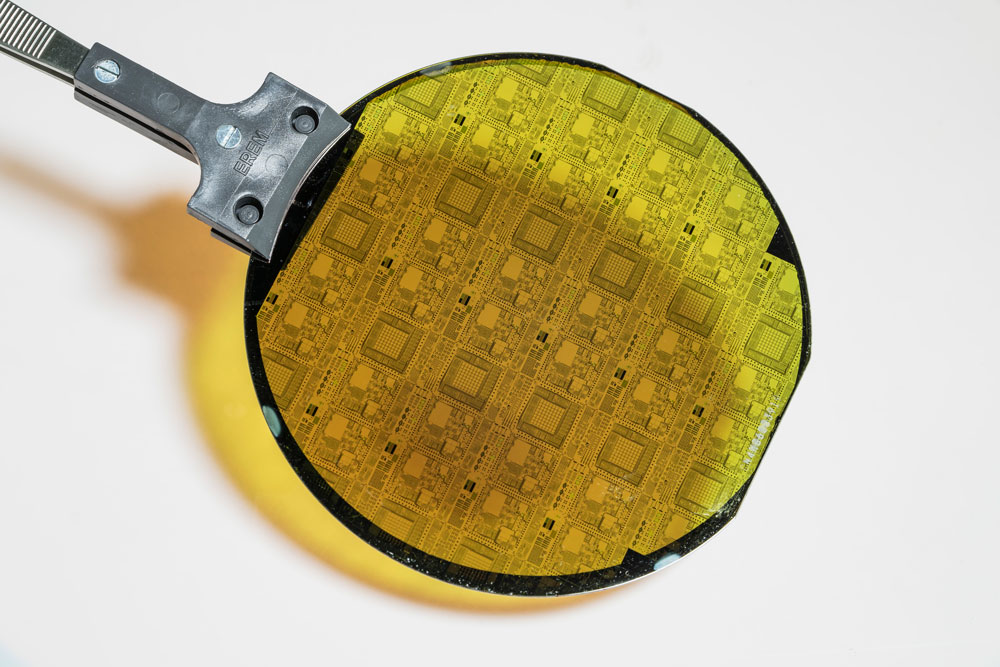
IISB offers two rectangular standard die sizes for MPW runs, depending on customer design dimension:
1 – physical chip edge length 2,5 mm x 5 mm – corresponding max. design side length 2,35 mm x 4,85 mm
2 – physical chip edge length 5 mm x 5 mm – corresponding design side length in the range of 4,85 mm x 4,85 mm
A basic design kit including design rules, basic electrical device models for NMOS and PMOS transistors, and a process overview are available.
Design rule check, Electrical rule check and Layout-vs-Schematics functionality for Cadence will be provided with a preliminary device library prior to the tape-out date.
Customers will receive a total of 30 diced samples including electrical test data.
Basic packaging services are available for this early-access technology.