UMS offers high-perfomance 0.25μm GaN high-electron-mobility-transistor (HEMT), 0.15μm GaN HEMT and 0.1μm GaAs Low Noise pHEMT processes.
GH25 is a space evaluated 0.25 μm HEMT GaN-on-SiC substrate technology for very high-power application. With GH25 it is possible to design GaN HPAs, LNAs, switches, diodes, MMICs, power bars and multi-function components.
GH15 is a 0.15μm HEMT GaN-on-SiC substrate technology for very high-power application.
PH10 PHEMT GaAs process is optimized for the production of low noise, wideband and medium power amplifier MMICs. With PH10 it is possible to design LNAs, variable Gain and Medium Power Amplifiers, mixers and multi-functions TX &RX MMICs, automotive radars, Imaging sensors, Optical fibre communication and Instrumentations.
GaAs BES (Buried Epitaxial Schottky) is a 1µm Schottky diode process that features an extremely high cut off frequency, enabling diverse circuit designs, from RF power detectors to passive balanced mixers for radar signal analysis and astronomy signal detection beyond 300 GHz. It includes two metal interconnect layers, precision TaN resistors, high-value TiWSi resistors, MIM capacitors, air-bridges, and via-holes. Optimized for low conversion loss and high-volume MMIC production, BES is recommended for mixers, passive receivers, and power detectors in telecommunications, automotive collision avoidance radars, and space communication systems.
GaAs ULRC 20 (Ultra Low Resistance Conductor) enables versatile passive circuit designs, including accurate microwave filters, RF power combiners, microwave baluns, matching elements, and low-loss lines, as well as power bar input/output matching circuits. Optimized for reproducibility, power handling, low losses, and high-frequency performance, it supports high-volume, high-yield production. It is ideal for designing hybrid MMICs for amplifier modules in antenna transmitters and receivers for Radars, Telecommunications, and Space Communication systems.
Device offering: Transistors for RF and low noise amplification, transistors for switch, Schottky diodes, MIM capacitors, inductors, mm-Wave passive elements, TaN and HRW resistors, evaporated and electroplated metallization:
UMS Technologies | |
|---|---|
GH25 0.25µm GaN HEMT
| AlGaN/GaN on SiC, 100µm substrate thickness 4.5 W/mm power density Power FETs: Ids+: 1A/mm Gm: 290mS/mm Recommended Operating Bias up to 30V Life Time >20 years at 200°C Tj Power and low noise RF amplification up to 20GHz |
GH15 0.15µm GaN HEMT | AlGaN/GaN on SiC 70µm substrate thickness 4.2 W/mm power density Power FETs: Ids+: 1.45A/mm Gm: 405mS/mm Recommended Operating Bias up to 25V Life Time >20 years at 200°C Tj Power and low noise RF amplification up to 40GHz |
PH10|GaAs pHEMT | AlGaAs/InG on GaAs pHEMT 70µm substrate thickness Gm 750mS/mm (Vds=2.0V, Gm_max) Idss >220mA/mm (Vds=2.V, Gm_max) Vbds >6V, 3V operating voltage 2 metal interconnect layers TaN/TiWSi/GaAs resistors Application area: Low noise RF amplification up to 110GHz |
GaAs BES | 1.0 µm Schottky diode Fully optical process Typical Ft: 3THz TaN,TiWSi, GaAs resistors iM.I.M. capacitors Air bridges, Via-holes Space evaluated process according to ESA (EPPL) Verification Frontend tools and eDRC on the website provided by UMS |
GaAs ULRC-20 | Fully optical process M.I.M. capacitors Inductors Metallic resistors TaN and TiWSi resistors Via holes through the GaAs substrate Thick Au lines Optional coating compatible with plastic package |
Technical Details | |
Frontend tools | Virtuoso (Cadence) for layout ADS (Keysight) and MwO (Cadence) for simulations and layout |
Verification tools | Frontend tools and website |
Delivery | 16 untested samples in the GH25& GH15 technology. 20 untested samples in the PH10 technology in Gel-Pak. PCM data, including RF measurements is available on request. |
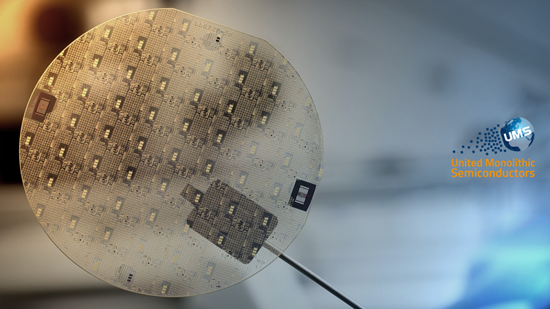
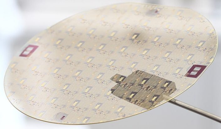
Wafer size | 4’’. The standard substrate thicknesses of 70μm and 100μm, depending on technology. |
Lead time | 4-5 months |