AMF

Technologies

CMC Microsystems announced that the organization will facilitate silicon photonics wafer runs through Advanced Micro Foundry (AMF) of Singapore with local European support from the EUROPRACTICE partner CMP (current CIME-P). In 2020, the Si-Photonics fabrication process AMF has become available for EUROPRACTICE customers.

AMF SI-PHOTONICS FABRICATION PROCESS

Technical characteristics:
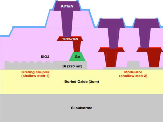
  • Silicon-on-insulator, 220-nm top Si film, 2000-nm buried oxide (BOX)
  • High resistivity handle wafer (>750 ohm-cm)
  • 193-nm deep UV lithography for waveguides, enabling features down to approximately 140 nm
  • Two partial etches and one full etch of the top silicon
  • 6 implants for optical modulators (P++, P+, P, N++, N+, N)
  • Germanium deposition and implanting for photodetectors
  • Two metal levels, no planarization
  • Front side oxide etch to selectively expose waveguides, e.g. for sensing applications
  • Deep trench with etched facets for edge coupling
  • Supports design and fabrication of a range of components and systems consisting of:

     – modulators

     – detectors

     – waveguides (strip or ridge)

     – gratings for fiber coupling

     – deep trench and nano-tapers for edge coupling

     – multiplexers (diffraction or arrayed waveguide) and filters (resonators, Bragg gratings)

     – ring and disk resonators.

  • Frontend Backend tools: Siemens EDA Pyxis and Luceda IPKISS-Tanner L-Edit