TEEM PHTONICS

Technologies

Teem Photonics

If silicon is one of the main materials used by the integrated photonics industry – because it reuses the manufacturing processes in force in the microelectronic area – glass is also the subject of all attention thanks to its optical characteristics: its transparency for visible to infrared wavelengths, its low refractive index, and its linear optical properties indeed allow, in comparison with silicon, to benefit from numerous advantages at the component scale, the reduction of input/output channels footprint, better performance for passive functions, the opportunity to operate in the visible area, and greater temperature stability.


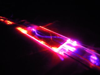
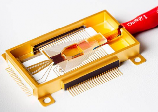
By developing a process to manufacture waveguides on glass, branded ioNext, and based on an ion-exchange reaction, Teem Photonics gives EUROPRACTICE users the opportunity to take advantage of glass assets by having a wide variety of passive components – available in a design kit that can be used through the free access design software NAZCA – to design and manufacture photonics circuits combining routing, filtering and coupling functions.
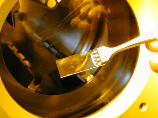
 

In addition, EUROPRACTICE users are also offered access to the WAFT (for Wave-guide Array to Fiber Transposers), glass interposers which are inserted between a silicon-photonics chip and an optical fiber array to ensure between these two elements a single-mode, wideband adiabatic transition, with a coupling loss of less than 0.5dB and a significant reduction in the input/output channels footprint.


Glass-photonics chip manufacturing

Light passing through a glass-photonics chip

Packaging of a silicon-photonics chip using WAFT

The ioNext platform adds two types of components which are entirely specific to it:

  • Mode Field Diameter (MFD) converters to guarantee a low-loss coupling with optical fiber and, at the same time, low-footprint on-chip functions;
  • surface waveguides to allow for the interaction of light with the chip surroundings, and thus to form the probe of an optical sensor.

You can find more technical details in the ioNext PIC brochure

Glass-photonics IC ioNext-NIR
Technology Characteristics
Process:
Based on a local exchange of doping ions to define gradient-index waveguides at the wafer-level
Uses 60mm diameter glass wafers (will increase to 100mm soon)
Requires only one photolithography step
Operating range:
Bandwidth from 1520 to 1570nm On-chip MFD of 4.2 x 3.2µm2
MFD converters at chip facet to match optical fibers’ MFD.
Performance:
Propagation loss of 0.15dB/cm at 1550nm Minimum radius of curvature of 800µm
Building blocks
Interconnects:
Straight waveguide
Arc bend
S-bend
Optical functions:
I/O port
Spot size converter
Surface waveguide
50/50 splitter
50/50 directional coupler
Waveguide crossing
Mach-Zehnder interferometer
Evanescent coupling
Coming soon (in the course of 2021):
Polariser
Multiplexer
Filter
Application area
Telecom and Datacom
Optical sensing
Microscopy and inspection
Software tools
NAZCA (free and open-source framework dedicated to photonics IC design)
Turnaround time
1 month between the gds transmission and the chip delivery
Glass-photonics IC ioNext-NIR
Technology Characteristics
Process:
Based on a local exchange of doping ions to define gradient-index waveguides at the wafer-level Uses 60mm diameter glass wafers (will increase to 100mm soon) Requires only one photolithography step
Uses 60mm diameter glass wafers (will increase to 100mm soon)
Requires only one photolithography step
Operating range:
Bandwidth from 650 to 800nm
Mode field diameter compatible with SM630 fiber
Performance:
Propagation loss of 0.3dB/cm at 780nm
Radius of curvature of 30mm (for the moment)
Building blocks
Interconnects:
Straight waveguide
Arc bend
S-bend
Optical functions:
I/O port
50/50 splitter
Crossing
Application area
Microscopy
Spectroscopy
Optical sensing and inspection
Software tools
NAZCA (free and open-source framework dedicated to photonics IC design)
Turnaround time
1 month between the gds transmission and the chip delivery

Two types of Wave-guide Array to Fiber Transposers (corresponding to the two silicon photonics coupling configurations) are available:

  • edge-coupling WAFT, designed to butt-couple with silicon-photonic chip facets, featuring a wideband transmission and handling both polarization states;
  • top-coupling WAFT, which provide full multichannel compatibility with grating couplers usually found on silicon-photonics chip.

Teem Photonics also makes its fiber pigtailing know-how available to EUROPRACTICE users by assembling both its WAFT and customized photonic chips with fiber arrays, thus offering lab-ready components.

Glass-photonics IC ioNext-NIR
Technology Characteristics
Process:
Based on the ioNext-NIR glass-photonics platform
Operating range:
Operating wavelengths from 1200 to 1700nm
Number of channels from 1 to 256
127µm or 250µm input pitch
Output pitch down to 20µm
Compatibility with both coupling modes (edge couplers and grating couplers)
Various type of fiber connection:
Single Mode (SM) or Polarization Maintaining (PM) fibers
FC, SC, ST or MPO connectors
Performance:
Max insertion loss: < 1dB
Max polarization-dependant loss: < 0.2dB
Max adjacent crosstalk: < -25dB
Application area
Photonic integrated circuits testing and characterization
Photonic integrated circuits packaging
Wafer-level testing of photonic components
Datasheets