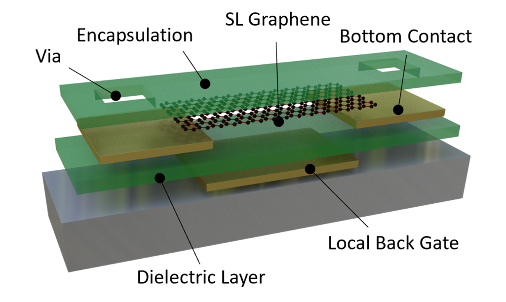
This MPW run of the 2D-PL project is mainly intended towards electronics but can also include sensor devices (e.g. Hall sensor, but via opening on graphene is not in the scope of this run) and will be provided by AMO GmbH. The design of the device can be adjusted within the specifications. The offered device structure is the GFET shown in the following image.

Parameter | Value | |
|---|---|---|
Graphene Mobility | >1000 cm²/Vs | |
Avg. Sheet Resistance | n=-5 x 1012 cm-2: | ~1 kΩ
|
Avg. Contact Resistance | n=-5 x 1012 cm-2: | ~1 kΩ µm |
Minimum working devices | >80 % | |
Dirac point | -10V … +10V | |
Safe gate-source voltage range | ± 20 V |
Substrate
Resolution
General design rule: 10 μm for in-layer critical dimension and over-layer alignment.
Layer thicknesses | |||
|---|---|---|---|
0 | Rigid Substrate | Si/SiO2 | 90 nm |
1
| Back Gate Contact | Ti/Pd or Ti/Au | 5 nm /40 nm |
2 | Dielectric Layer | Al2O3 | 40 nm |
3 | Bottom Contact | as layer 1 | 5 nm /40 nm |
4 | Graphene | Single layer, CVD on Cu | |
5 | Encapsulation | Al2O3 | 40 nm |
6 | Bondpads | Au | 300 nm |
Characterization