Through the 2D Pilot Line (2D-PL), users can access Graphenea’s Process Flow 2. The same process flow, together with Process Flow 1 and Process Flow 3, is available directly via imec.
Would you like to know the best path for you? Please, contact Chiara Mancini.
Graphene is an atomically thin material, with properties that enable novel devices and technologies unachievable with conventional semiconductors such as silicon, germanium or compound materials. With Graphenea, you can prototype and develop graphene-based solid-state devices for applications in biosensing, optoelectronics and photonics.
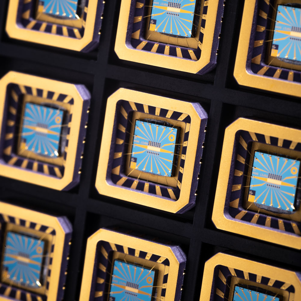
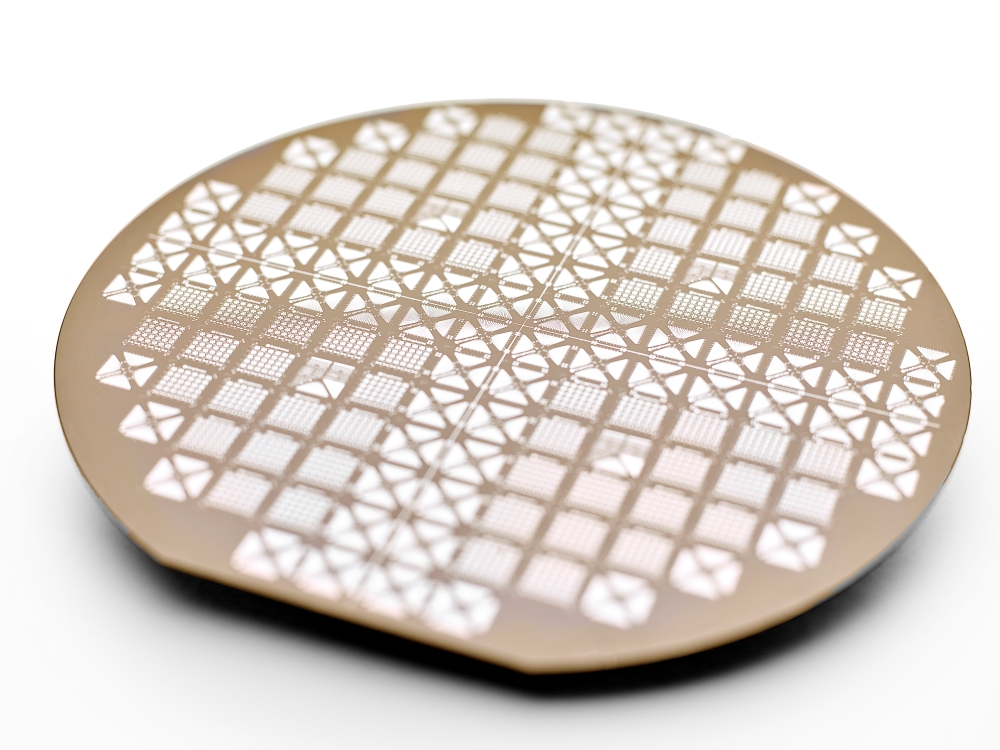
Graphenea uses semiconductor manufacturing techniques to produce graphene-based devices at the wafer scale, such as resistors, capacitors, diodes, Hall sensor elements and field effect transistors. The foundry has three distinctive process flows that allow to fabricate these discrete components and even combine some of these devices within a single die, enabling the fabrication of simple circuitry.
Graphenea’s proprietary fabrication processes enable them to guarantee metrics in their runs, ensuring the customer’s devices are up to standards. Moreover, short manufacturing cycles use far less resources compared to those of traditional silicon, reducing the amount of water, gases and other chemicals and materials, significantly reducing their carbon footprint.
Process Flow 2 is tailored for liquid sample measurements, offering features particularly suited for biosensing and liquid biopsies. The passivated contacts prevent large leakage currents and device degradation upon contact with the liquid analyte, enabling measurements in saline solutions, as well as biological fluids like blood, plasma, saliva, and sweat.
Graphenea Process Flow 2 – Biosensing | |||
|---|---|---|---|
Transistors | CVD-graphene
gated through substrate | Ambipolar FET p-type at VG=0 | Width=10µm Length=10µm |
Resistors | CVD-graphene | p-type, 1kOhm/sq | Width=10µm Length= 10µm |
Substrate | SiO2/Si | SiO2=90nm Si=525µm | |
Metal contacts | Au | CD=10µm Thickness = 50nm | |
Encapsulation | Al2O3 | CD=10µm Thickness = 30nm | |
Via opening | CD=10µm | ||
QC | Carrier transport | In PCM dies | Mobility >1000cm2/V·s Dirac Point<20V Hysteresis<10V |
Raman | In PCM dies | Raman · I(G)/I(2D) < 1.25 · I(D)/I(G) < 0.15 · Pos(G) < 1600 cm-1 · FWHM(2D) < 45 cm-1 | |
Optical | In PCM dies | Channel integrity > 95% Device yield within die > 75% | |