

Graphene offers unique properties that can potentially surpass the capabilities of silicon photonics enabling next-generation photonic devices. The integration of graphene with traditional semiconductor platform is a key step towards the commercialisation of solutions based on 2D materials. In the framework of 2D-PL Project several experimental multi-project wafer (e-MPW) runs are provided where universities, research institutes and companies can include their designs as dies on joint wafers.
IHP – Leibniz Institute for High Performance Microelectronics, focuses on the development of graphene photonic integrated circuits (PIC) in a 200 mm pilot line. This involves exploring various integration aspects for the realization of integrated devices. The process flow is based on graphene photonic module on 200 mm Si wafers and enables a fabrication of proof-of-concept devices like graphene electro-absorption modulators, Mach-Zehnder interferometers or micro ring resonators. Design rules will include the basic design elements to be used in this particular e-MPW run.
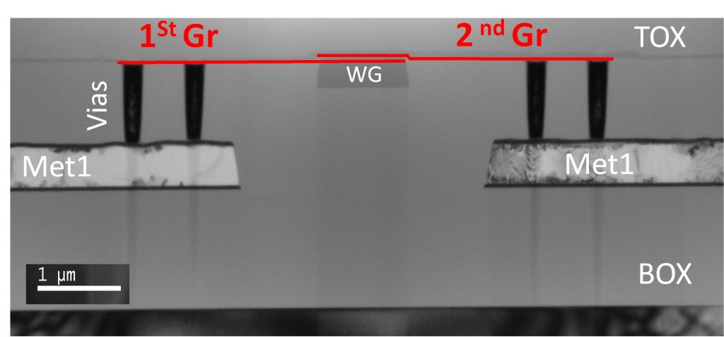
The e-MPW process flow is built on Dual Layer graphene electro-absorption modulator flow. The process includes essential modules such as contact, waveguide, and coupler modules, along with specialized graphene integration for enhanced functionality. Cladding and encapsulation modules ensure optical confinement and device protection. Finally, metal heaters could be implemented in the flow.
Process Step | Process/Layer | Material | Thickness |
|---|---|---|---|
0 | Bottom Cladding (BOX)
| SiO2
| 1200 – 2600 nm
|
1
| Met1 Layer | Ti/TiN/AlCu/Ti/TIN | 480 – 530 nm |
2 | Oxide layer and CMP
| SiO2
| |
3 | Waveguide | SiN | 400 nm
|
4 | Via opening | ||
5 | Grating coupler | SiN | |
6 | Graphene Layer | CVD Monolayer Graphene | |
7 | Spacer Layer | SiN | 20-40 nm |
8 | Graphene Layer | CVD Monolayer Graphene | |
9 | Passivation Layer | SiN | 20 nm |
10 | Top Cladding | SiO2 | 500 – 2100 nm
|
11 | Pad opening | ||
12 | Top Heaters | Various Metals | 20-60 nm |